Thin-Film Alchemy: The Microscopic Revolution from Atoms to Chips (Part III)
Physical Vapor Deposition (PVD) for Thin-Film Fabrication
Physical Vapor Deposition (PVD) is a technique for depositing thin films via physical processes, commonly used for metal film deposition.
PVD encompasses three primary technologies: Vacuum Evaporation, Sputtering, and Molecular Beam Epitaxy (MBE).
1.Vacuum Evaporation
In the early days of thin-film technology, metal films were predominantly formed through physical evaporation. Today, vacuum evaporation is primarily employed for metal deposition in discrete components or low-integration-density circuits.
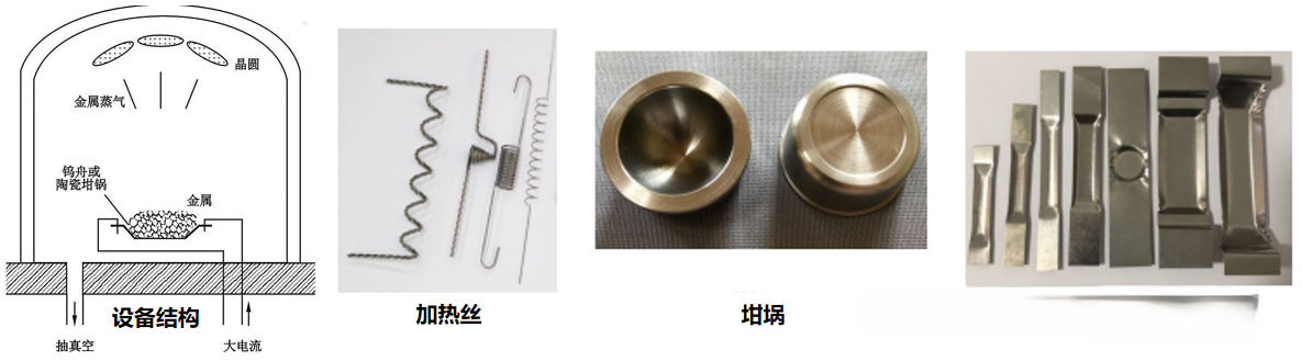
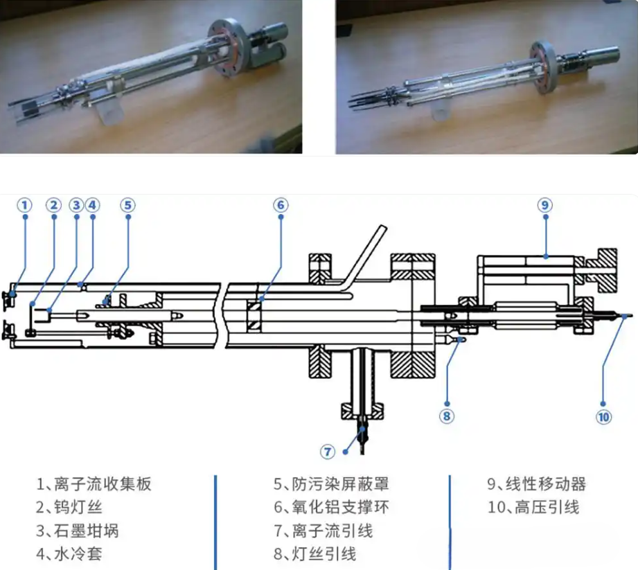
Principle of Vacuum Evaporation
In a high-vacuum environment (approximately 10⁻³ Pa to 10⁻⁶ Pa), the target material (e.g., metals, alloys, or organic compounds) is vaporized into gaseous atoms or molecules through methods such as resistive heating, electron beam bombardment, or laser heating. These vaporized species then migrate through the vacuum and condense onto the surface of a low-temperature substrate, forming a thin film.
Advantages
The equipment is simple and cost-effective, with a high deposition rate.
It offers high purity, as the vacuum environment minimizes impurity contamination.
It is suitable for large-area uniform deposition, especially for materials with high vapor pressure (such as pure metals like gold, silver, and aluminum).
Disadvantages
Weak adhesion: The bonding between the film and substrate is primarily due to van der Waals forces, requiring pretreatment (e.g., roughening, intermediate layers).
High directionality: The evaporation source is point- or surface-based, causing film thickness to vary with the substrate's distance and angle relative to the source; uniformity depends on fixture design.
Difficulty in depositing low-vapor-pressure materials (e.g., tungsten, ceramics) and alloys (compositional deviation occurs due to differing evaporation rates of components).
Sputtering
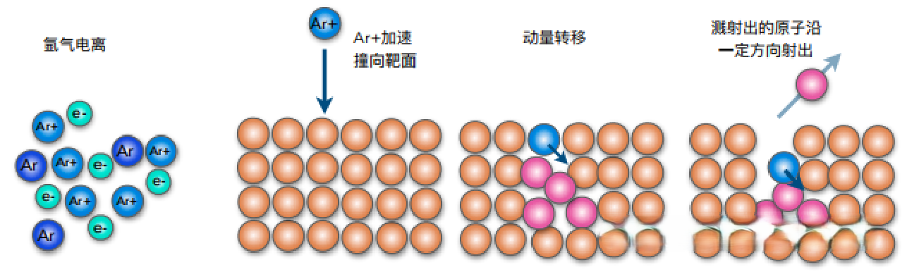
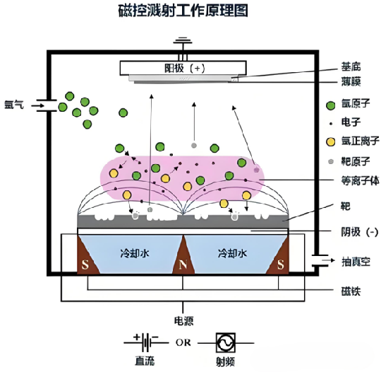
Sputtering is a physical vapor deposition (PVD) method in which a plasma bombards a target material, causing its atoms or molecules to be ejected and deposited onto a substrate to form a thin film.
n a low-vacuum environment (approximately 10⁻¹ Pa to 10⁻³ Pa), an inert gas is introduced into the high-vacuum reaction chamber to facilitate gas discharge. Under a high-voltage electric field, the gas ionizes, generating a large number of ions. These ions are accelerated by the electric field, gaining high energy and bombarding the target material at high speed. When the kinetic energy of the ions exceeds the binding energy of the target material's atoms or molecules, the target atoms or molecules are ejected. These ejected particles then travel toward the substrate and deposit on its surface, forming a thin film.
Advantages
Broad material compatibility: Capable of depositing metal alloys, ceramics, insulators (via RF sputtering), and even compounds (via reactive sputtering, e.g., introducing O₂ to produce oxide films).
High film quality: High particle energy (10–100 eV) results in dense films with strong adhesion, and composition closely matches the target material (especially beneficial for alloys).
Excellent uniformity: Magnetic fields homogenize the plasma, enabling large-area deposition (e.g., wafers, glass substrates).
Disadvantages
Complex and costly equipment: Requires a sputtering power supply, vacuum system, and gas control setup.
Lower deposition rate: Typically in the nanometer-per-second to nanometer-per-minute range (slower than vacuum evaporation), with potential gas impurity incorporation (e.g., argon atoms embedded in the film).
Molecular Beam Epitaxy (MBE)
Molecular beam epitaxy is a physical deposition method conducted in an ultra-high vacuum system. The constituent elements of the thin film are heated to generate directional molecular beams, which are then directed toward a temperature-controlled substrate, where they deposit and form a thin film.
n an ultra-high vacuum environment (<10⁻⁸ Pa), elemental or compound source materials are heated to a gaseous state, forming collimated atomic/molecular beams. These beams are deposited onto a precisely temperature-controlled single-crystal substrate at an extremely low rate (approximately one atomic layer per second). Through lattice matching, epitaxial growth is achieved, ensuring the thin film maintains the same crystal structure or an ordered arrangement as the substrate.
Advantages
Atomic-level precision: Film thickness, composition, and doping can be controlled down to a single atomic layer, resulting in minimal defects.
Heterostructure fabrication: Enables growth of ultra-thin multilayers (e.g., GaAs/AlGaAs quantum wells) with abrupt interfaces (<1 nm).
Low growth temperature: Avoids substrate diffusion or defects caused by high temperatures, making it suitable for thermally sensitive materials.
Disadvantages
High cost and complexity: Requires ultra-high vacuum systems, multi-source control, and in situ monitoring equipment.
Extremely slow deposition rate (~a few nanometers per minute), limiting it to small-area substrates (lab-scale wafers).
High technical barriers: Demands stringent substrate surface cleanliness and temperature uniformity.
AMTD provides high-precision Showerhead services for core components, with products mainly including Showerhead, Faceplate, Blocker Plate, Top Plate, Shield, Liner, Pumping Ring, Edge Ring, and other core components of semiconductor equipment. These products are widely used in the semiconductor, display panel, and other fields, with excellent performance and high market recognition.