Thin-Film Alchemy: The Microscopic Revolution from Atoms to Chips (Part IV)
Metallization and Planarization
Metallization involves the formation of a metal film through methods such as vacuum evaporation or sputtering, followed by photolithography and etching to delineate the metal film into interconnects, which are crucial for realizing device functionality.
Planarization is the process of flattening the uneven dielectric layers on the wafer surface. After planarization, the dielectric layer exhibits minimal height variations, facilitating the subsequent fabrication of the second layer of metal interconnects with improved pattern accuracy.
Metallization
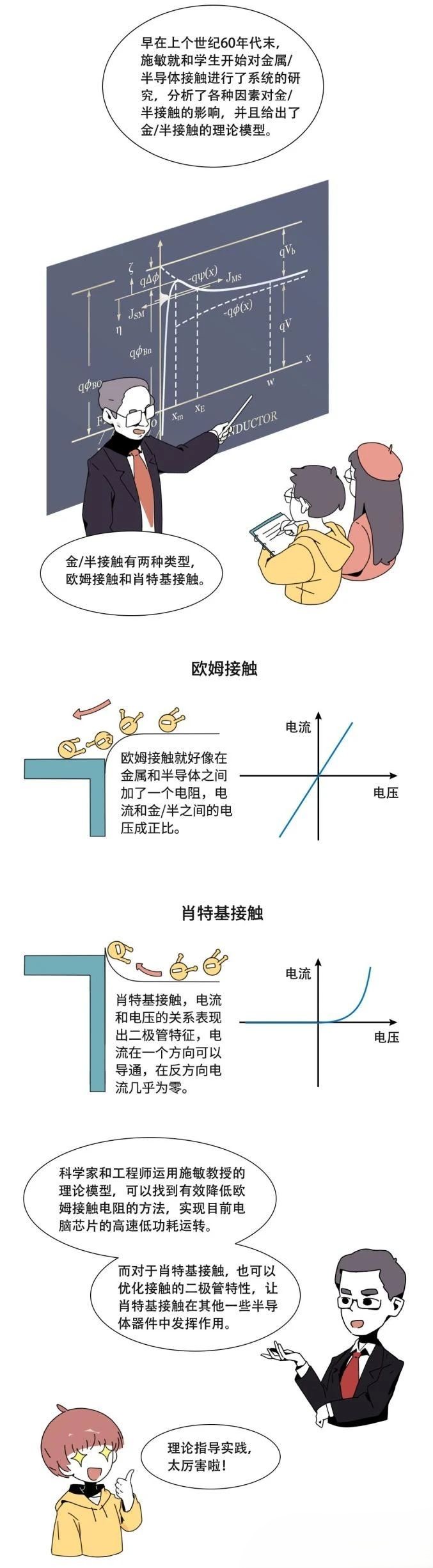
If a metal is simply connected to a semiconductor without proper treatment, a rectifying effect (Schottky barrier) will occur at the contact region. This undesired unidirectional conductivity prevents transistors or integrated circuits from functioning properly. To eliminate this rectifying effect, an Ohmic contact must be formed.
Ohmic Contact
A high-quality ohmic contact must meet the following requirements:
① Linear and symmetric current-voltage relationship – The voltage and current should exhibit a linear and symmetrical characteristic.
② Low contact resistance – The contact should introduce minimal additional impedance.
③ Mechanical robustness – It must withstand external stresses such as impact and vibration.
There are three primary methods to form an ohmic contact:
Heavily doped semiconductor ohmic contact
Low-barrier-height ohmic contact
High-recombination-center ohmic contact
Heavily Doped Semiconductor Ohmic Contact
In device fabrication, the heavily doped semiconductor method is commonly employed. The probability of electron tunneling is strongly influenced by the barrier height, which in turn depends on the doping concentration at the semiconductor surface. A narrower barrier enhances tunneling effects, and the barrier width is determined by the doping concentration—higher doping leads to a thinner barrier.
By precisely controlling the doping concentration, an effective ohmic contact can be achieved. When the doping concentration exceeds 10¹⁹/cm³, the surface barrier becomes sufficiently thin, allowing carriers to tunnel through easily, thus forming an ohmic contact. The contact resistance in this method varies with doping concentration.
Low-Barrier-Height Ohmic Contact
A low-barrier-height ohmic contact is essentially a Schottky contact, such as the interface between platinum and p-type silicon. Ideally, if the metal's work function is greater than that of p-type silicon but less than that of n-type silicon, an ohmic contact can form. However, due to interface states at the metal-semiconductor junction, a space charge region and a contact barrier may develop. Consequently, when the semiconductor's surface doping is low, achieving a near-ideal ohmic contact becomes challenging.
High-Recombination-Center Ohmic Contact
When the semiconductor surface has a high density of recombination centers, current transport between the metal and semiconductor is primarily governed by these centers. A high recombination center density significantly reduces contact resistance, resulting in nearly symmetric current-voltage characteristics. Under these conditions, an ohmic contact can form between the semiconductor and metal.
As microelectronic devices continue to shrink in feature size while wafer dimensions increase and integration levels rise, interconnect and contact technologies face ever-higher demands.
Beyond forming reliable ohmic contacts, interconnect materials must meet the following criteria:
Low resistivity and high stability
Fine-pattern etchability and resistance to environmental degradation
Good film deposition properties, strong adhesion, and excellent step coverage
High electromigration resistance and good solderability
Alloying Process
The alloying method, also known as the sintering method, can be used not only to form ohmic contacts but also to fabricate PN junctions. During the alloying process, metal is placed on the wafer, loaded into a mold, and pressed tightly before being heated in a vacuum above its melting point. The molten alloy dissolves and solidifies with the wafer, forming an ohmic contact upon completion. The entire process consists of three stages: heating, constant-temperature holding, and cooling.
Planarization
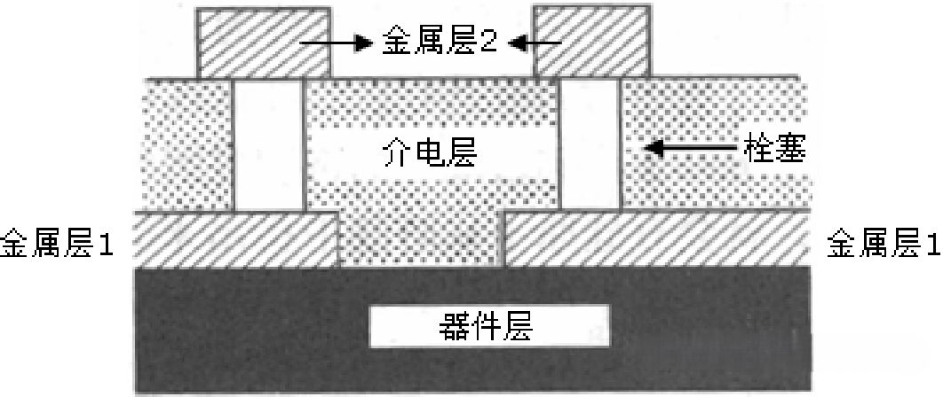
As the integration density of integrated circuits increases, the wafer surface can no longer provide sufficient area for the required interconnects. Particularly for highly complex products such as microprocessors, multiple layers of metal interconnects are needed to link various components within the chip. This has led to the development of double- and multi-layer interconnects.
In multi-layer interconnect structures, except for via plugs, direct contact between metal layers must be avoided to prevent short circuits. Therefore, insulating layers must be used to isolate adjacent metal layers.
The dielectric material used to separate metal layers is called the intermetal dielectric (IMD) layer. The fabrication of IMD layers involves multiple processes such as sputtering, CVD, photolithography, and etching. Achieving a planar dielectric layer is challenging and often prone to void formation. Additionally, as the metal layer surface becomes increasingly uneven, the deposited dielectric layer also exhibits topography variations. This unevenness makes photolithography exposure focusing difficult for subsequent metal layers, affecting pattern transfer accuracy and complicating the etching process.
With the inevitable adoption of multi-layer interconnects in IC manufacturing, planarization has emerged as a critical enabling technology.
Common dielectric materials include:
Borophosphosilicate glass (BPSG)
Silicon dioxide (SiO₂)
Silicon nitride (Si₃N₄)
Among these, SiO₂ is the most widely used due to its excellent insulating properties and process compatibility.
Planarization techniques include:
1. Etch Back (Reverse Etching)
2. Glass Reflow
3. Spin-On Films
4. Chemical Mechanical Planarization (CMP)
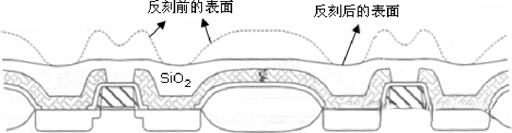
Reverse Etch-Back Method
The reverse etch-back method involves initially depositing a sacrificial layer to fill the cavities and recesses on the wafer surface. Subsequently, dry etching techniques are employed to etch away the sacrificial layer. By utilizing an etching rate that is faster for the protruding (higher) features compared to the recessed (lower) ones, a planarization effect is achieved. The etching process continues until the material to be etched reaches its final desired thickness, while the sacrificial layer material still remains within the recesses on the wafer surface.
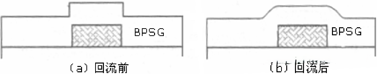
Glass reflow involves heating doped silica glass (such as a material containing dopants) at high temperatures to induce its flow, thereby achieving local planarization. For instance, when borophosphosilicate glass (BPSG) is annealed in a nitrogen atmosphere at a temperature of 850°C, its fluidity enables it to achieve planarization and also fill cavities or holes.
Spin-on coating is a technique that applies various liquid materials onto the wafer surface through spinning to achieve planarization, primarily used for device planarization and gap filling in 0.35μm and larger technology nodes. The planarization effectiveness depends on factors such as solution composition and molecular weight. Materials for spin coating may include photoresist, doped silicon dioxide, or various resins.
After spin coating, baking is conducted to evaporate the solvent, leaving silicon oxide to fill lower gaps. To further fill surface gaps, an additional layer of silicon oxide can be deposited using CVD methods. Chemical Mechanical Planarization (CMP) achieves surface flattening through relative motion between the wafer and polishing head, preferentially removing elevated features at a faster rate than lower patterns to obtain a planar surface.
An abrasive slurry is applied between the polishing head and wafer, where controlled pressure enables interaction between the abrasive and wafer surface to achieve planarization. CMP offers high polishing precision and is currently the most widely used planarization technology in the industry.
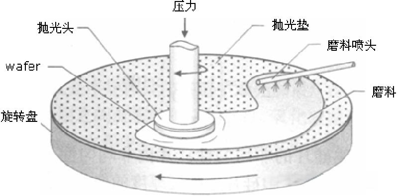
The abrasive slurry and polishing pad are consumables in the polishing process, and they significantly impact the quality of chemical mechanical polishing (CMP), requiring strict control. (The abrasive slurry is a mixture of abrasive particles and chemical reagents. Common types include oxide slurry, tungsten slurry, and copper slurry. Oxide slurry, used for oxide dielectric polishing, is a potassium hydroxide or ammonium hydroxide solution containing ultra-fine silica particles. Tungsten slurry uses alumina powder or silica as abrasive particles. Copper slurry requires the addition of a compound of ammonium hydroxide and alumina, which is then ground by abrasive particles.)
In chemical mechanical planarization, the polishing pad is a critical component that determines the polishing rate and degree of planarization. Polishing pads are typically made of polyurethane, which exhibits sponge-like mechanical elasticity and water-absorption properties. The micropores in the polishing pad aid in slurry distribution and polishing uniformity. After polishing a certain number of wafers, the pad surface becomes smooth and flat, reducing its ability to control particles and decreasing the polishing rate. Therefore, polishing pads must be replaced periodically during use.
AMTD provides high-precision Showerhead services for core components, with products mainly including Showerhead, Faceplate, Blocker Plate, Top Plate, Shield, Liner, Pumping Ring, Edge Ring, and other core components of semiconductor equipment. These products are widely used in the semiconductor, display panel, and other fields, with excellent performance and high market recognition.