


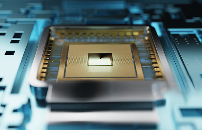
In the semiconductor industry, even the tiniest defect can lead to the scrapping of an entire batch of wafers. Building a full-chain quality control system from raw materials to final delivery, with a "zero-defect" philosophy embedded in every m
Time:2026-05-19

In the field of semiconductor equipment core components, the Showerhead is merely the starting point. The complete product matrix built around the gas distribution system is the true reflection of an enterprises comprehensive strength. Three Types, Precis
Time:2026-05-19

In semiconductor coating equipment, the temperature uniformity across the wafer surface directly affects thin-film consistency and chip yield. As the core component of temperature control, the heaters design quality determines the upper limit of the proce
Time:2026-05-19

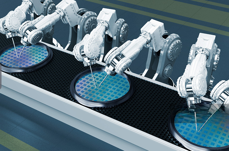
Quality control for semiconductor equipment components must cover the full spectrum — from microscopic film layers to macroscopic dimensions. The establishment of a comprehensive inspection system is the fundamental guarantee that every product leaving th
Time:2026-05-19
In the semiconductor equipment components field, capacity and precision are often a contradiction. AMTD, with its plan to "introduce over 140 high-precision machining equipment in phases," delivers an answer that balances both efficiency and pre
Time:2026-05-19

The welding quality of semiconductor equipment components directly determines product reliability under extreme conditions such as high temperature, vacuum, and corrosive gases. Building a comprehensive welding technology platform covering multiple high-e
Time:2026-05-19

In semiconductor equipment, the surface treatment quality of components directly affects the corrosion resistance, wear resistance, conductivity, and cleanliness of the final product. Surface treatment may appear to be a "back-end process," but
Time:2026-05-19
In semiconductor fabrication processes, uniform gas distribution directly determines the quality and consistency of thin-film deposition. The Showerhead, also known as a gas distribution plate or gas shower plate, is precisely the core device in this crit
Time:2026-05-19

|
Address:No. 29 Nanhai Road, Yi'an District, Tongling City, Anhui Province |

|
Email:SHD@Ferrotec.com.cn |

|
Tel :021-31340912 |


