


The shift from planar SoCs to 3D-ICs and advanced packaging requires thinner wafers to enhance performance and reduce power, thereby shortening the distance signals need to travel and the energy required to drive them.
Demand for ultra-thin wafers is on the rise. The total thickness of an HBM module containing 12 DRAM chips and a base logic chip is still less than that of a premium silicon wafer. Thin wafers play a crucial role in assembling fan-out wafer-level packaging (FOWLP) and advanced 2.5D and 3D packaging for AI applications, which are growing much faster than mainstream ICs. Coupled with the industry's demand for lightweight and thin mobile phones, wearables, and medical electronics, it seems that modern microelectronics would be impossible without the ability to reliably process thin silicon wafers.
The reveal process for thin silicon vias (TSVs) is a classic process that requires back-side processing. "Almost any stacked device must have silicon vias," says Rick Reed, Senior Director of 3D/Advanced Technology at Amkor Technology. "Introducing silicon vias in many current applications requires a very controlled thinning process, and since you almost always need to perform back-side processing, the process immediately requires temporary bonding and debonding processes."
The first step in any wafer thinning process is to determine the target. "If there are what we call blind TSVs in the silicon, and you don't know the depth range of all TSVs in the wafer, then you risk grinding into some of them," Reed explains. "Since copper diffuses quickly in silicon, this can cause leakage. But it can also contaminate the grinding wheel, so subsequent wafers will have copper on them."
Several key decisions need to be made during the thinning and processing of thin device wafers. Which temporary adhesive is most compatible with the process flow? Can it hold the thin wafer in place during various processes, including CMP and high-temperature deposition, and be cleanly removed after processing? Which carrier wafer is best suited for the application, silicon or glass? Among several leading methods, which debonding process can best remove the adhesive after processing at a reasonable cost?
Despite the security provided by carrier wafers (also known as handle wafers), ultra-thin wafers are fragile and delicate. This makes them susceptible to damage, including micro-chipping and cracking during the thinning process and subsequent high-temperature processes such as plasma-enhanced chemical vapor deposition (PECVD). When ultra-thin wafers undergo photolithography patterning, PECVD, reflow, dicing, and debonding (carrier removal), damage is the biggest threat to yield. Additionally, other issues may arise due to warpage between wafers and/or void formation.
"In terms of yield and wafer thinning, everything revolves around controlling the wafer edge thinning process," says Thomas Rapps, Product Manager at Suss. "Delamination can occur not only during the grinding process but also during thermal processing. Furthermore, if there is some internal stress in the device wafer, it can easily warp. Therefore, delamination may be caused by warpage or some kind of void between the two wafers, which you can inspect for, but eventually, cracks will appear."
The edge of the wafer is rounded at the bevel, but after thinning, this profile changes. "So, if you're grinding a device wafer, you usually end up with a very sharp tip, ideally just one atom in thickness," Rapps says. "It's extremely fragile. Edge chipping means that a part of the edge breaks off, which can also trigger a crack that runs through the entire wafer. Therefore, to prevent this from happening, you usually perform edge trimming, which also requires the use of a grinding wheel. You need to cut a step on the wafer edge, with a depth at least as deep as the final wafer thickness."
In addition to managing basic yield issues, chipmakers are also seeking customized solutions for their specific device types, with tool reliability being the top requirement. "The applications of device complexity are becoming more and more specific," says Ian Latchford, Director of Product Marketing at Lam Research. "Customers need precision and want a repeatable process every time. They don't want a general solution, but they want a solution that works the same way every time and has high productivity."
To meet these needs, the industry is refining thinning steps, adhesives and removal chemicals, as well as temporary bonding and debonding processes (see Figure 1). Adhesives, typically organic thermosetting or thermoplastic materials, are spin-coated onto the carrier wafer, while thinner debonding materials are usually spin-coated onto the device wafer. Bonding is performed under vacuum thermal compression (TCB) or via UV irradiation. The carrier wafer provides a base for the thinning and processing of the device wafer until the removal chemical is involved in the debonding process.
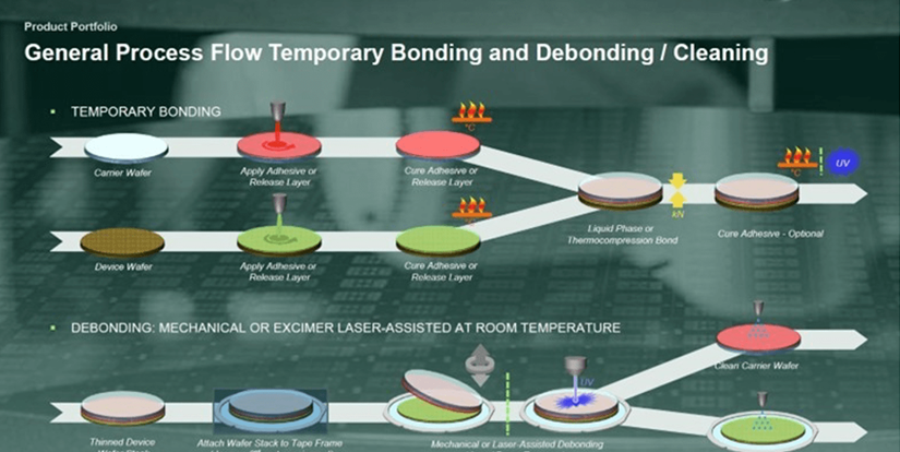
Figure 1: Temporary Bonding (Top) and Debonding (Bottom) Process Flow
Silicon vs. Glass Carrier Wafers
The industry employs both glass and silicon carrier wafers. One reason glass has emerged as a popular carrier is that its Coefficient of Thermal Expansion (CTE) can be engineered to closely match that of silicon, ensuring compatibility with other materials in the stack. For instance, borosilicate glass exhibits a CTE similar to silicon, remains stable over a wide temperature range, and can transmit infrared (IR) or ultraviolet (UV) lasers through its surface to activate debonding release layers.
Hamed Gholami Derami, Business Development Engineer at Brewer Science, states: "For mechanical debonding and infrared laser debonding, either silicon or glass carriers may be used depending on process requirements. However, for UV laser and photonic debonding, glass carriers are mandatory."
Part of the appeal of silicon carrier wafers lies in their compatibility with all wafer processing tools and electrostatic chucks. Silicon's CTE perfectly matches that of silicon devices. A final advantage of silicon is its ability to achieve lower Total Thickness Variation (TTV) more cost-effectively compared to glass wafers.
Thomas Uhrmann, Chief Technology Officer at EV Group, remarks: "When comparing glass and silicon carriers of equivalent quality (i.e., same TTV), the cost difference can be nearly double."
How Temporary Bonding Works
When stacking one wafer temporarily onto another, engineers typically employ a carrier wafer, an adhesive or temporary bonding adhesive, and a release layer that facilitates easy removal after processing. In rare cases, a single adhesive layer may perform both functions. Crucially, the bonding and debonding mechanisms must work synergistically to enable clean removal of the processed material from the carrier after debonding.
Adhesives are evaluated based on multiple criteria. They must bond at low temperatures yet withstand high-temperature processing. The adhesive must be uniformly deposited across a 300mm surface via spin coating while achieving high bonding uniformity.
The ideal adhesive would bond at low temperatures and then remain bonded throughout backside processing and thinning," says Paul Lindner, Executive Technical Director at EV Group. "It should withstand extremely high temperatures without degrading or altering its properties. We want release at room temperature with low force, so there's no additional thermal budget. Most importantly, the adhesive should have excellent thickness uniformity, which stems first from coating uniformity and then from bonding uniformity, as any thickness non-uniformity would lead to non-uniform backside grinding of the product wafers and often cannot be easily compensated in backside grinding.”
However, what works for one application may not suit another. "The main issue is that there's basically no one-size-fits-all solution for all possible processes," says Rapps of Suss. "The most important criterion for material selection is temperature stability. What's the maximum temperature between temporary bonding and debonding in the downstream process? Many materials can reach 250°C because if you do reflow, you typically don't need to go higher than that. But only a few materials can reach 350°C."
Spin coating offers a degree of process flexibility. "With spin coating, you can planarize the material so it can also embed certain features, such as microbumps that need to be soldered later," Rapps says. "Therefore, the adhesive has two functions—it acts as an adhesive, but it can also planarize embedded features with very low or very high topography. So after spin coating, we bake the wafers and then bond them together. Curing the material to stabilize the bond is often required, but this is actually material-solution specific."
Wafer Thinning Priorities
Next, the wafer undergoes gradual thinning. Reducing thickness to below 100µm requires a delicate balance of grinding, CMP, and etching processes to meet stringent Total Thickness Variation (TTV) specifications—the difference between the thickest and thinnest measurements on the wafer. For silicon, this is typically measured using a laser interferometer at hundreds of points across the wafer, with TTV being a critical quality metric that must be maintained wafer-to-wafer and lot-to-lot in high-volume manufacturing.
Thinning a wafer is akin to sanding wood. Starting with coarse grinding, progressively finer abrasives are used to achieve the smoothest possible final result. For wafers, each step enhances wafer-to-wafer uniformity and reduces TTV.
The roughest method is the wafer grinding step, which results in final thickness variations in the range of a few micrometers," explains Mattias Nestler, Director of Products and Technologies at scia Systems. "The CMP step is more precise than wafer grinding, achieving variations in the hundreds of nanometers. Next, using plasma etching, we can reach 10 to 100 nanometers. Or, with ion beam etching as a final step, in the best case, we can trim the wafer 20 times, so a 250-nanometer variation can be reduced to 25 nanometers. We can use a two-step trimming process with measurements in between for even better results.
Given the importance of total thickness variation, engineers are keen to quantify the sources of variation during thinning and processing. "We use a glass carrier to reveal the TSVs, but even the best glass you can buy has a TTV of only 1 micrometer across the entire wafer," says Reed of Amkor. "Then, when we apply adhesive on top, this adds a few micrometers of variation. Our grinding process is very uniform but still introduces about 2 micrometers of TTV.”
Dry etching also introduces variations, which can be radially distributed. "So when you add it all up, you're looking at variations of around 5 micrometers," Reed says. "Our TSV reveal Six Sigma process is very robust, handling these sources of variation by carefully setting up and understanding the depth variations of the TSVs from the start."
Techniques to Ensure Precision in TSV Reveal Processes Include:
Mapping the depth of TSVs defined by Bosch etching in silicon;
Uniformly spin-coating adhesive and release layers, followed by baking, curing, and bonding;
Backgrinding the silicon using coarse, medium, and fine grinding steps to within 10 micrometers of the TSV bottom, achieving a mirror-like finish;
Coarse, medium, and fine CMP (Chemical Mechanical Polishing);
Employing plasma etching to expose the TSVs;
Depositing a silicon nitride film as a polishing stop layer;
Depositing a thick layer of silicon dioxide on top of the TSVs, followed by CMP to reveal the TSVs.
The functionality on the grinding wheel provides automatic feedback on the silicon thickness during the grinding process, and similar adaptive CMP processes can enable more successful and extreme thinning of the silicon," says Reed.
Another parameter requiring close monitoring is temperature. "We are now controlling the temperature of the CMP process in situ, which has numerous benefits for the CMP process overall," states Dan Trojan, CEO of Axus Technology. "The primary temperature constraint is the glass transition temperature of the polishing pad, which is made of polyurethane. When this temperature is exceeded, the polymer transitions from a liquid to a solid, and the friction becomes significantly higher, leading to rapid deterioration. Therefore, we have a method to essentially cool the surface of the processing pad without diluting the slurry, which also aids in improving the removal rate. We also employ a multi-zone membrane carrier to apply varying pressures locally on the wafer instead of applying a single pressure."”
Currently, the most common TSV architecture for silicon interposers may utilize TSVs with a diameter of 11 micrometers and a depth of 110 micrometers, with barrier metal and oxide insulating layers occupying 1 micrometer of that diameter. While the fabrication of, for example, 5-micron TSVs with a depth of 55 microns has been demonstrated, the industry currently appears to favor the use of thicker, more expensive 100-micron silicon interposers.
The most common challenge engineers face in thin-wafer processes is preventing defects or microcracks, particularly at the wafer edges.
Selective plasma etching applied only at the wafer edges helps remove edge defects, while selective CVD can passivate the edges. "In the field of 3D packaging, stacked wafer structures require something to fill the gaps at the edges," says Latchford of Lam Research. "Due to CMP roll-off causing gaps, device manufacturers have encountered many issues with edge profiles. They then have to thin down the device wafers, which may ultimately lead to edge cracking, significantly impacting yield. Therefore, we actually place micron-scale silicon dioxide films here to fill the gaps in bonding wafer flow applications.
Plasma etching or ion beam etching processes can also eliminate any defects induced during the CMP process, such as subsurface scratches, so-called pits (indentations in the silicon lattice), and stains.
Finding the Right Release Method
For debonding, UV and IR laser ablation, as well as photonic debonding, have emerged as leading mechanical separation mechanisms due to their compatibility with large thin-wafer formats (300 mm wafers, 50 µm thick) and their ability to separate wafers with minimal device damage compared to thermal sliding and chemical immersion methods (see Figure 2).
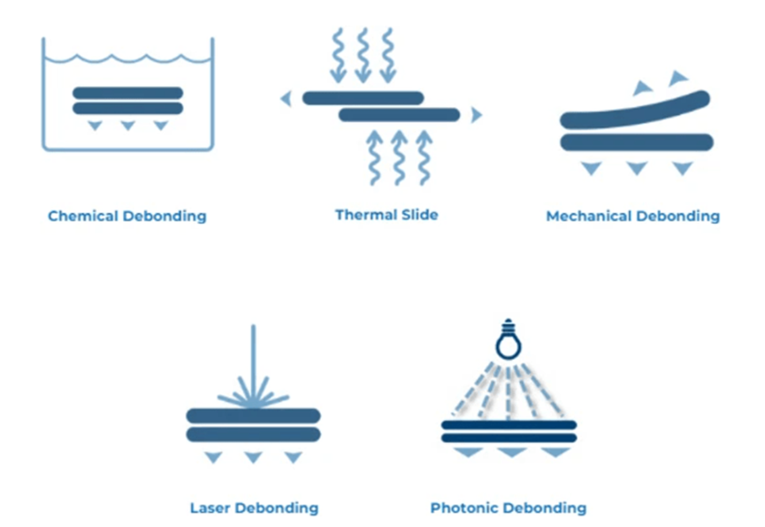
Figure 2: Most Popular Wafer Debonding Methods
Thermal sliding debonding utilizes polymers with lower melting points, known as thermoplastics, which flow when heated to facilitate sliding and separation. Unfortunately, this method is incompatible with thermal processes like PVD of metals or PECVD of dielectrics, which generate significant wafer stress and may lead to wafer cracking. Thermal sliding also exposes devices to more thermal cycles than necessary, as competing debonding methods operate at room temperature. Nevertheless, thermal sliding debonding remains a low-cost option and a viable choice for smaller, slightly thicker substrates.
Chemical dissolution works by immersing the bonded pair in a solvent, and perforating the carrier wafer can help accelerate the process. High solvent consumption and low yield have hindered the widespread adoption of chemical debonding.
Chemical debonding materials were used in older packages and relied on chemical baths to release the wafer," says Derami of Brewer Science. "Thermal sliding materials were later introduced and are still used in some processes, but they have limitations in terms of the minimum wafer thickness they can handle, thermal budget, and yield. On the other hand, with mechanical debonding, we can handle thinner wafers with lower stress levels, easier debonding, and a better thermal budget, making it suitable for high-temperature applications. More recently, laser debonding materials offer the most flexibility. They can handle thinner wafers with higher yields and near-zero force debonding.
Photonic debonding is a relatively new debonding method that uses pulsed broadband light sources to debond temporarily bonded wafer pairs by employing a light-absorbing layer as an inorganic metallic release layer. One advantage of photonic debonding is its lower cost and faster production speed compared to laser ablation methods, along with high tolerance to variations in focal distance to the release layer. This makes it compatible with bonded pairs that have some curvature or bowing. For applications that thin substrates below 20 µm and use very high downstream temperature processes where adhesion and TTV control are critical, photonic debonding may be the preferred debonding method.
Mechanical debonding, also known as mechanical peeling, uses a blade inserted between the wafer pair to physically separate them. This method requires device wafers that can withstand some physical pressure
Laser ablation employs UV lasers (254, 308, or 355 nm) or IR (1064 nm) lasers along with a release layer tuned to that wavelength, working by absorbing the illumination energy, undergoing a chemical change, and separating. It is the fastest debonding method, processing about 20 to 30 wafers per hour, with minimal stress on the wafer. However, a shielding layer may be required to mitigate any damage to the devices caused by laser acoustic waves. For applications that thin substrates to below 20 µm and use very high downstream temperature processes where adhesion and TTV control are critical, laser debonding is the preferred debonding method.
Sometimes the bottleneck of the system is not the actual debonding step but the removal of the adhesive after debonding," says Lindner of EVG. "This wet processing step dissolves the adhesive, so if the adhesive remains on the carrier, it can be taken off and processed elsewhere. But if the adhesive remains on the product, there are often multiple cleaning modules working in parallel to match the throughput of the debonding module.
In recent years, EVG has developed a nanocleaving method where inorganic layers replace organic adhesives. Such inorganic layers in silicon can withstand higher temperatures (>900°C) and are thus compatible with all front-end processes. The company anticipates its use not only in advanced packaging but also in front-end layer-stacking applications.
Translation
As architectures requiring temporary bonding and debonding processes become more prevalent, the industry's demand for recycled carriers - particularly silicon carrier wafers - continues to intensify. This has introduced a series of challenges
If certain chemicals are used, they may come into contact with the carrier material and corrode it, leading to degradation over time,' said Suss's Rapps. 'However, typically carriers can be used up to 10 times as part of optimizing costs for high-performance and high-value devices.
Conclusion
Wafer thinning, temporary bonding, thin wafer handling, and debonding methods are becoming indispensable process steps in 2.5D and 3D packaging, wafer stacking, and wafer-level fan-out packaging. Chip manufacturers are collaborating closely with suppliers to select appropriate adhesives, debonding materials, bonders, debonding methods, grinding, CMP, etching, and cleaning processes for producing ultra-thin devices with thicknesses below 50µm while maintaining high yields and reliability. This requires thermal stability, mechanical stability, and meticulous attention to wafer edges - all critical factors in mitigating potential defects and improving yields when implementing these essential thin wafer processes. AMTD is an emerging technology enterprise dedicated to the R&D, manufacturing, and sales of advanced semiconductor devices. The company has established comprehensive systems for showerhead technology development, surface treatment, micro-hole machining, precision welding, and quality control. These capabilities enable AMTD to deliver innovative solutions widely applied in semiconductor fabrication, display panel production, and other high-tech industries.


