


Nanotechnology is a highly interdisciplinary field that involves the precise control and manipulation of matter at the nanoscale. Integrated circuits (ICs), as a crucial technology that has reached the nanoscale, have had a profound impact on society and daily life. The critical dimensions of transistor devices have continuously shrunk over the past few decades, now approaching 10 nanometers or even smaller. This technological advancement allows for more devices to be packed onto each chip, enabling more powerful computing capabilities, higher storage capacities, and faster operating speeds.
What is Nanotechnology?
The U.S. National Nanotechnology Initiative (NNI) provides a broad definition of nanotechnology, describing it as "the manipulation of matter at the atomic or molecular scale, where at least one dimension is on the order of 1 to 100 nanometers." This definition does not elaborate on the potential or specific applications of nanotechnology, deliberately so, as the focus of the definition is to provide guidance from a size perspective. A more easily understandable definition might be: the ability to create products with practical value and real-world applications using simple and inexpensive basic building blocks—atoms and molecules.
To put the nanoscale into perspective: the diameter of a water molecule is about 0.1 nanometers, a glucose molecule is roughly 1 nanometer in diameter, a typical virus measures about 100 nanometers in diameter, while the diameter of a human hair is approximately 105 nanometers, and the diameter of a baseball is around 108 nanometers. Therefore, the lower limit of nanotechnology, around 1 nanometer, corresponds to the size of basic molecules in nature.
He Development Journey of Nanotechnology: From Conception to Practical Application
The development journey of nanotechnology embodies the crystallization of human wisdom and the relentless pursuit of scientific exploration.
The Germination of Theoretical Conceptions
The theoretical foundation of nanotechnology can be traced back to 1959, when Richard Feynman, a Nobel Laureate in Physics, first systematically explored the possibility of manipulating matter at the atomic scale in his lecture titled "There's Plenty of Room at the Bottom". In his lecture, Feynman proposed numerous forward-looking ideas, including high-density integrated circuits, microscopes capable of observing atomic-level structures, and microscopic robots for drug delivery. Looking back at history, these conceptions have been realized in the development of modern computer chip technology, electron microscopes, and intelligent drug delivery systems, proving the value of Feynman's far-sighted vision.
The formal coining of the term "nanotechnology" is attributed to Professor Norio Taniguchi from Japan. In 1974, he used this term to describe thin-film manufacturing technologies in the semiconductor field that were precise down to the ten-nanometer scale, such as physical vapor deposition processes. However, the introduction of this term did not initially garner widespread attention, and its true popularization occurred much later.
In 1986, Eric Drexler published the book "Engines of Creation: The Coming Era of Nanotechnology," which significantly broadened the dissemination of the concept of "nanotechnology." Inspired by Feynman's lecture, Drexler proposed many imaginative concepts in his book, such as storing the entire Library of Congress in a space the size of a sugar cube or constructing objects at the atomic scale using molecular machines. Although some scientists regarded these ideas as science fiction-like fantasies, the book undoubtedly stimulated thinking and discussion within the scientific community and among the public about the potential of nanotechnology.
Breakthroughs and Development of Key Technologies
Substantial progress in nanotechnology stems from scientific breakthroughs in multiple core technologies. As early as the 1960s and 1970s, advancements in patterning and imaging technologies laid the foundation for design and manufacturing at the nanoscale. Although the electron microscope was invented by Ernst Ruska and Max Knoll in 1931, the technology developed slowly over the subsequent decades, primarily limited to laboratory research. It wasn't until 1961 when Möllenstedt and Spiedel from the University of Tübingen successfully produced lines with widths of less than 100 nanometers using electron beam lithography, laying the groundwork for subsequent technological developments.
During the same period, several researchers began exploring the application of electron beam lithography in the manufacturing of microelectronic devices. In 1960, Selvin and McDonald from Sylvania Electronic Systems published the article "The Future of Electron Beam Techniques in Microelectronic Circuits"; the following year, O. Wells from the Westinghouse Research Laboratories also published a study titled "Electron Beams in Microelectronics," further advancing the theoretical development in this field.
Milestones
The 1980s witnessed several significant breakthroughs in the field of nanotechnology. In 1981, Binnig and Rohrer invented the Scanning Tunneling Microscope (STM) at the IBM Zurich Research Laboratory. This innovation made it possible to observe individual atoms for the first time and earned them the Nobel Prize in Physics in 1986. In the same year, Binnig and his team also successfully developed and operated the Atomic Force Microscope (AFM), further expanding the capabilities of nanoscale observation.
Notable progress was also made in the field of materials science. In 1985, the Kroto team discovered fullerenes, an achievement that later won the Nobel Prize in Chemistry in 1996. In 1991, Sumio Iijima from NEC Corporation discovered carbon nanotubes in the soot of an arc discharge apparatus. Subsequently, in 1992, Harrington and Maganas from Maganas Industries successfully synthesized carbon nanotubes using the Chemical Vapor Deposition (CVD) process, driving further development in this field.
A landmark event in the history of nanotechnology occurred in November 1990, when Donald Eigler and Erhard Schweizer from the IBM Almaden Research Center used a Scanning Tunneling Microscope to arrange individual xenon atoms on a nickel surface to spell out the word "IBM". This marked the first public demonstration of the ability to manipulate individual atoms and became an important milestone in the history of nanotechnology development.
Nanomanufacturing: Top-Down, the Art of "Sculpting"
He implementation of nanotechnology typically employs one of two main approaches: the top-down method. This method involves a series of manufacturing processes and techniques to gradually sculpt, shape, and ultimately form nanoscale components from larger materials.
The manufacturing process of the top-down method is closely related to the processes commonly used in the integrated circuit (IC) and microsystem industries. Its core technologies include:
· Thin film deposition: Depositing a thin film on the surface of a material, with a thickness typically ranging from a few to several tens of nanometers.
· Lithography: Utilizing photosensitive polymers to generate the desired structural patterns through patterning processes.
· Etching processes: Chemically or physically treating the areas generated by lithography to remove unwanted parts, thereby forming the final structure.
Taking Figure 1 as an example, it demonstrates the application of these technologies in the manufacturing process of nanoscale mechanical resonator devices. This field widely adopts the top-down method to precisely construct complex structures, highlighting its irreplaceable role in high-precision manufacturing.
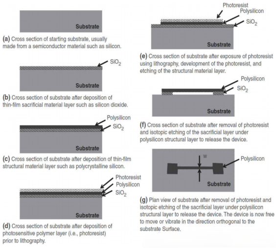
Figure 1: Process Flow Diagram for Nanomechanical Resonator Manufacturing Using Top-Down Nanotechnology Approach
(a) Cross-section of the starting substrate, typically made of a semiconductor material such as silicon.
(b) Cross-section of the substrate after deposition of a thin film sacrificial material layer (e.g., silicon dioxide, SiO₂).
(c) Cross-section of the substrate after deposition of a thin film structural material layer (e.g., polysilicon).
(d) Cross-section of the substrate after deposition of a photosensitive polymer layer (i.e., photoresist) prior to lithography.
(e) Cross-section of the substrate after exposing the photoresist using lithography, developing the photoresist, and etching the structural material layer.
(f) Cross-section of the substrate after removing the photoresist and releasing the device by isotropically etching the polysilicon structural layer underneath the sacrificial layer.
(g) Plan view of the substrate after removing the photoresist and releasing the device by isotropically etching the sacrificial layer underneath the polysilicon structural layer. At this point, the device can move or vibrate freely in the direction perpendicular to the substrate surface.
Substrate (基底), SiO₂ (Silicon Dioxide, 二氧化硅), Polysilicon (多晶硅), Photoresist (光刻胶)
The entire manufacturing process starts with a substrate typically made of monocrystalline silicon. Current semiconductor substrates have achieved extremely high flatness and smoothness, which are crucial characteristics for fabricating nanoscale components. Next, a thin film layer known as the "sacrificial layer" is deposited. This layer is not used in the final device but serves as a support between the resonator and the substrate, and will be removed at the end of the manufacturing process. Common sacrificial materials include thin films of silicon dioxide (SiO2). Subsequently, another thin film layer called the "structural layer" is deposited, which will be used to form the resonator. A typical structural material is polysilicon (also known as "poly-Si").
There are various processes available for depositing these thin film layers, such as chemical vapor deposition (CVD), physical vapor deposition (including sputtering and evaporation), atomic layer deposition (ALD), spin coating, and molecular beam epitaxy. Some of these techniques are also classified as "bottom-up" nanotechnologies.
Before patterning, a layer of photoresist, a light-sensitive material, is applied to the thin film, usually through a spin-coating process. Then, electron beam lithography (e-beam) technology is used to pattern the thin film. Immediately afterwards, dry plasma reactive ion etching is employed to process the structural layer and etch out the desired shape. The photoresist is subsequently removed through a plasma ashing process, while the "sacrificial layer" is removed using a vapor-phase etchant (such as vapor-phase hydrofluoric acid). The completion of this process allows the structural layer to achieve free mechanical motion, ultimately forming a complete nanoscale resonator device.
As shown in Figure 1, the cross-section and plan view of the resonator clearly present the key characteristics of its manufacturing process, such as the width of the resonator labeled as "w". However, it should be noted that Figure 1 only illustrates one application scenario of the "top-down" approach and is not the exclusive process for manufacturing all nanodevices.
To date, the most well-known and commercially highly successful application of the "top-down" approach may be found in the most advanced integrated circuits,In integrated circuits, FinFET transistor technology is employed. FinFET, short for Fin Field-Effect Transistor, is a non-planar metal-oxide-semiconductor (MOS) transistor technology widely used in the most advanced microprocessors today. The core dimension of this type of transistor is the gate length, and currently, the gate length of mass-produced FinFET technology on the market has reached the 3-nanometer scale.
Note: The "nanometer" figures in modern chip manufacturing are more of a marketing term and do not fully correspond to the actual physical dimensions of the gate. The same numerical node may represent different actual feature sizes among different manufacturers. The actual physical gate length is usually larger than the value named in the process node.
Here are some reference data: For the 14nm process node, the actual gate length is approximately 20-25nm; for the 7nm process node, it is about 16-18nm; for the 5nm process node, it is around 14-16nm; and for the 3nm process node, it is approximately 12-14nm.
The core feature of FinFET lies in its unique three-dimensional structure. Its core component is a single-crystal silicon fin structure that stands upright from the substrate surface, with a high aspect ratio, as shown in Figure 2. Specifically, Figure 2b presents a three-dimensional schematic of the FinFET device topology, clearly illustrating the structure of this type of transistor.
imilar to traditional MOS transistors, FinFETs also consist of a source, a drain, and a gate. However, the difference lies in the fact that the source and drain are connected through a narrow silicon fin with a high aspect ratio (height greater than width). This fin not only serves as a channel for charge carriers (electrons or holes) to flow from the source to the drain, but the flow of carriers within it is also regulated by the gate potential.
The position and design of the gate are also highlights of FinFETs. As shown in Figure 2a, the gate material is composed of a layer of conductive material that overlaps the fin on three sides (top and both sides), known as a "tri-gate structure". However, a very thin layer of dielectric material separates the fin and the gate, which maintains effective control of the carriers while preventing the possibility of direct electrical contact. This three-sided overlapping design significantly enhances the ability of the gate voltage to control the carriers in the fin, thereby greatly improving transistor performance.
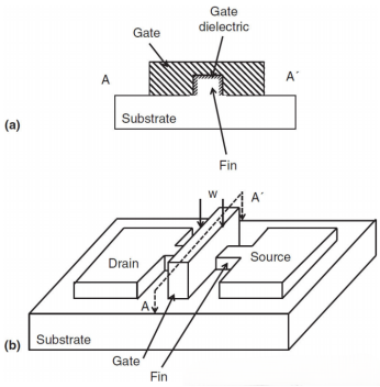
Figure 2: Schematic diagram of a FinFET transistor.
Figure 2b presents a three-dimensional representation of a single-fin FinFET transistor. The source, drain, and fin are all made of single-crystal silicon. The fin serves as a high-aspect-ratio channel connecting the source and drain, through which charge carriers can flow. As shown in Figure 2a, the fin is coated with a thin layer of gate dielectric, followed by a layer of gate material, which is typically a conductive material. Due to the electric field generated by the gate voltage from both sides and the top, this structure is also known as a tri-gate transistor.
(Terminology translation:
Gate -> 栅极
Gate dielectric -> 栅极介质
Substrate -> 衬底
Fin -> 鳍片
Drain -> 漏极
Source -> 源极)
The gate length (indicated by "w" in Figure 2) is one of the important parameters characterizing FinFETs. In the most advanced FinFET technology currently available, the gate length has reached 14 nanometers. One of the greatest advantages of this structure is its ability to enhance the "on" current by increasing the number of fins, thereby further improving transistor efficiency. Additionally, the unique design of FinFETs paves the way for higher packaging density.
Intel first proposed the idea of using this innovative FinFET technology to extend Moore's Law when they introduced the 22-nanometer Ivy Bridge microprocessor. They pointed out that traditional transistor architectures were no longer sufficient to achieve the 22-nanometer node, necessitating a breakthrough in design. The success of the FinFET structure not only achieved this goal but also drove the evolution of process technology towards 14-nanometer and even smaller nodes.
The FinFET structure is just one of many successful examples of "top-down" nanotechnology. In fact, there are many other tools and methods used to manufacture nanoscale devices, and new technologies are being developed and applied every year. However, it should be noted that top-down approaches typically do not achieve atomic-level precision control, meaning that certain extreme applications may have to turn to other technological paths.
Nanomanufacturing: Bottom-up Approach, Building Blocks from Molecules
The second major method for implementing nanotechnology is the "bottom-up" approach. This technological pathway essentially involves the engineering process of gradually assembling atoms or molecules into objects with nanoscale or even larger structures. This method is renowned for its high control precision and design flexibility. One of its core ideas is to design molecules with specific shapes and molecular recognition capabilities, enabling these molecules to self-assemble automatically under appropriate conditions, thereby forming preset system configurations.
A typical example of the bottom-up approach is Atomic Layer Deposition (ALD). ALD is a highly precise thin-film deposition technique, with the key lying in its sequential and self-limiting gas-phase chemical reaction process. In this process, reactive gases known as "precursors" react with the target surface in a self-limiting manner, thereby building up thin films of material layer by layer.
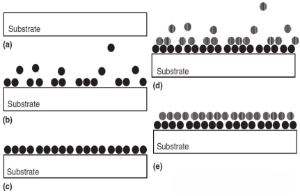
In a typical ALD process, two precursor gases are usually used, and they are not introduced into the deposition chamber simultaneously. The entire process is divided into multiple steps that cycle as follows:
Figure 3a: First, the substrate is placed into the reaction chamber, which is the starting point for thin-film deposition. Figure 3b: The first precursor gas is introduced, which reacts chemically with the substrate surface to form a monomolecular layer of a chemical species. Figure 3c: After the first layer reaction is complete, the excess precursor gas in the reaction chamber is removed. Figure 3d: Subsequently, the second precursor is introduced, which reacts with the monomolecular layer of the first precursor to form a new monomolecular layer. Figure 3e: After the second reaction is complete, the remaining gas is removed again.
This chemical reaction cycle can be repeated any number of times as needed to ultimately achieve precise control over the film thickness.
Compared with traditional Chemical Vapor Deposition (CVD) methods, ALD has a significant advantage in that its deposited layers exhibit excellent conformality and uniformity, while the film thickness can be controlled with extremely high precision. Various materials can be deposited using ALD, including SiO2, Al2O3, ZrO2, HfO2, TiN, etc. Among these, high-k dielectric materials (such as HfO2) have become the preferred material for the gate dielectric layer in FinFET transistors in modern integrated circuits.
However, despite its numerous advantages, ALD also has drawbacks that cannot be ignored, primarily manifested as a relatively low deposition rate. This characteristic necessitates efficiency optimization for large-scale production.
Among the many examples of the bottom-up approach, the most famous cases are carbon nanotubes and other carbon-based molecules in the fullerene family. These materials occupy an extremely important position in nanotechnology due to their exceptional structures and properties.
Manufacturing of Carbon Nanotubes
Carbon nanotubes are an allotrope of carbon, mainly classified into single-walled nanotubes and multi-walled nanotubes. Their structural forms include concentric tubular shapes (the so-called "Russian doll model") and rolled-up "parchment models". As shown in Figure 4, the various allotropes of carbon also include diamond, graphite, fullerenes, and C60 carbon fullerene molecules (also known as "buckyballs"). Among these, single-walled carbon nanotubes typically have a diameter of about 1 nanometer, and their length-to-diameter ratio can reach an astonishing 132,000,000:1.
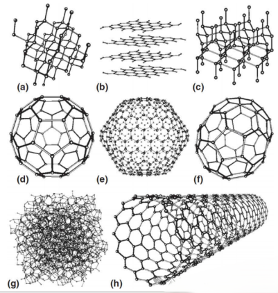
Figure 4. Schematic diagram of several different allotropes of carbon molecules, including (a) diamond, (b) graphite (single-atom-layer molecular carbon), (c) lonsdaleite, (d) C60 or buckyball (platinum fullerene), (e) C540 fullerene, (f) C70 fullerene, (g) amorphous carbon, and (h) single-walled carbon nanotube.
Carbon nanotubes exhibit many superior material properties. For example:
Mechanical properties: Carbon nanotubes have extremely high tensile strength (13 to 53 GPa) and elastic modulus (1 to 5 TPa), coupled with a low density, resulting in a specific strength of up to 48,000 kN·m·kg⁻¹, the highest among known materials. Carbon nanotubes exhibit many superior material properties. For example: Mechanical properties: Carbon nanotubes have extremely high tensile strength (13 to 53 GPa) and elastic modulus (1 to 5 TPa), coupled with a low density, resulting in a specific strength of up to 48,000 kN·m·kg⁻¹, the highest among known materials.
Vrious methods have been developed for the preparation of carbon nanotubes, including arc discharge, laser ablation, and chemical vapor deposition (CVD). Among these, the CVD method has attracted considerable attention due to its great potential for large-scale production.
During the CVD process, it is typically necessary to deposit a layer of suitable catalyst material on the substrate surface or pattern the catalyst at specific locations, so that carbon nanotubes will grow in the regions where the catalyst is present. Commonly used catalysts include nickel, cobalt, iron, or combinations of these materials. Importantly, the size and type of carbon nanotubes are influenced by the diameter of the catalyst particles on the substrate surface – smaller diameter catalysts will form single-walled nanotubes. By precisely patterning the position and diameter of the catalyst, the size, type, and location of the carbon nanotubes can be reasonably controlled.
The process of growing carbon nanotubes by CVD includes the following steps:
1. Heat the substrate to approximately 700°C. 2. Introduce process gases (such as ammonia, nitrogen, or hydrogen) and carbon-containing gases (such as acetylene, ethylene, or methane) into the reaction chamber. 3. Carbon nanotubes start to grow from the metal catalyst sites on the substrate surface.
If an electric field is applied in the deposition chamber, the growth direction of the carbon nanotubes will be oriented along the direction of the electric field, allowing for the growth of vertically aligned carbon nanotubes from the catalyst sites. This structure is observed, for example, when using plasma-enhanced CVD technology. Furthermore, under some special conditions, vertical alignment can be achieved even without an electric field, as long as the distribution of catalyst sites is sufficiently dense. Additionally, the combination of water-assisted CVD technology with catalysts has been shown to significantly increase the growth rate.
Production of Graphene
Among the numerous novel carbon-based materials, graphene is being developed to replace traditional semiconductor materials (such as silicon) due to its exceptional properties. Graphene, as a two-dimensional allotrope of carbon, exists in a sheet structure that is a single atom thick, with carbon atoms arranged in a honeycomb lattice. It possesses many remarkable characteristics, including ultra-strength, high thermal and electrical conductivity, and a nearly transparent appearance.
Regarding the structure of graphene, there are two main orientations: Zigzag orientation: always exhibits metallic behavior. Armchair orientation: its conductive properties depend on chirality and can manifest as either semiconducting or metallic.
Graphene has an extremely high electron mobility at room temperature, with reported values exceeding 15,000 cm²·V⁻¹·s⁻¹ and a theoretical limit as high as 200,000 cm²·V⁻¹·s⁻¹, which is tens of thousands of times higher than that of copper. Furthermore, its electron and hole mobilities are expected to be nearly symmetric. With these superior properties, graphene offers the possibility of significantly enhancing the performance of integrated circuits.
Research has shown that graphene can be successfully used to manufacture transistors. A typical example is the graphene field-effect transistor (FET) developed by the IBM research team, which demonstrates the enormous potential of graphene. The IBM team reported that the operating frequency of these transistors significantly increases as the device size decreases. For instance, they measured a cutoff frequency of 26 GHz for a graphene transistor with a gate length of 150 nanometers, setting a record for graphene FETs.
He development of graphene exemplifies the enormous potential of carbon-based materials in achieving high-performance integrated circuits. However, nanotechnology is still in its early stages of development, and with the continuous emergence of new materials, manufacturing processes, and device designs, its future development potential is immeasurable.
In addition to graphene, some other two-dimensional materials have also shown remarkable potential. For example, researchers at the Swiss Federal Institute of Technology (ETH) have designed integrated circuits using molybdenite (composed of molybdenum disulfide, MoS₂) that is only one atom thick.
Molybdenite stands out due to its nanostructure, which is similar to that of graphene. Specifically, in its multilayer form, molybdenite behaves as an indirect bandgap semiconductor, whereas in its monolayer form, its properties shift to those of a direct bandgap semiconductor. The reported mobility is approximately 200 cm²·V⁻¹·s⁻¹, with a current on/off ratio reaching 10^8 at room temperature.
Although many bottom-up approaches are still in the experimental stage, some technologies have already been used to produce carbon-based materials for practical applications. For instance: Fullerenes, which are molecular structures composed of carbon atoms, have attracted attention due to their spherical or tubular forms. Nanoparticles, such as silver and gold nanoparticles, have been incorporated into other materials to form composites with enhanced properties.
Manufacturing of Gold and Silver Nanoparticles
Silver nanoparticles are commonly prepared using wet chemical methods. For example, stable nanoparticle suspensions can be obtained by reducing silver nitrate (using sodium borohydride as a reducing agent) and adding colloidal stabilizers such as cellulose. These particles are often marketed for their antibacterial properties, claiming to effectively reduce external infections. However, authoritative medical research has not yet confirmed the therapeutic efficacy of this material.
Gold nanoparticles are typically generated by mixing chloroauric acid with a reducing agent. During this process, when a supersaturated state is formed in the solution, gold particles precipitate in nanoscale form, and stabilizers are added to prevent further aggregation of the particles. Gold nanoparticles have a wide range of applications in the biomedical field due to their unique physical and chemical properties. Although research and early applications have shown the potential of gold nanoparticles in the medical field, specific process optimization and large-scale production are still ongoing.
Nanotechnology Metrology
Nanotechnology metrology is a set of key technologies used for precise measurement and analysis of physical and chemical properties at the nanoscale. This field encompasses a variety of advanced measurement tools, including scanning tunneling microscopy (STM), atomic force microscopy (AFM), scanning electron microscopy (SEM), transmission electron microscopy (TEM), X-ray diffraction, and more. In this discussion, we will focus on STM and AFM, and information on other technologies can be found in relevant literature.
Scanning tunneling microscopy is an extremely precise instrument capable of scanning and imaging material surfaces at the atomic scale. The core component of STM is a tip probe with an extremely small radius (often just one atom wide), made of conductive materials such as tungsten, gold, or platinum-iridium, typically manufactured using wet etching processes.
The working principle of STM is based on the quantum mechanical tunneling effect. When the probe is brought close to the material surface to a tiny gap of approximately 5 to 10 angstroms, and a bias voltage (V_Bias) is applied between the probe and the sample, a tunneling current (I_tunneling) is generated. Using a closed-loop feedback circuit, STM can precisely measure the tunneling current passing through the probe and maintain a constant current by adjusting the distance between the tip and the surface (changes in the z-direction), thereby generating atomic-scale images of the material surface.
Remarkably, the intensity of the tunneling current exhibits an exponential relationship with the distance between the probe and the material surface. For every angstrom the tip moves closer to the surface, the tunneling current increases by a factor of 10. This grants STM an extremely high sensitivity, with a lateral (x, y-direction) resolution of up to 0.1 nanometers and a vertical (z-direction) resolution of 0.01 nanometers.
In addition to imaging, STM is also capable of spectroscopic analysis. By measuring the relationship between current and voltage (I-V curve), STM can reveal the electronic structure properties of surface atoms, making it a powerful tool for studying the physical and chemical behavior of surfaces.
Atomic force microscopy (AFM) operates on a fundamentally different principle from STM. AFM primarily uses a mechanical probe instead of an electrical one to scan the material surface. AFM relies on a sharp probe at the end of a cantilever, typically made of silicon and manufactured using micro-electro-mechanical systems (MEMS) technology. The scanning motion of the probe over the material surface is controlled by piezoelectric (or electrostatic) actuation.
When the probe approaches the material surface, according to Hooke's law, the cantilever will deflect due to the interaction forces between the surface and the probe. AFM is capable of measuring various surface forces, including mechanical contact forces, van der Waals forces, chemical bonding forces, Casimir forces, and capillary forces. The deflection of the cantilever is typically measured using a laser reflection system, where a laser beam is reflected from the top of the cantilever to a photodetector, precisely capturing the motion of the probe. Additionally, devices such as capacitive sensors can also be used for deflection detection.
AFM can also measure temperature, thermal conductivity, and other physical quantities using specialized probes, expanding its applications across multiple disciplines. Depending on the application requirements, AFM can operate in one of the following three modes:
Contact mode: The probe maintains direct contact with the sample surface, which is suitable for high-resolution scanning of rough surfaces.
Tapping mode: The probe vibrates rapidly on the surface, which is suitable for non-destructive scanning of flexible samples or larger areas.
Non-contact mode: The probe maintains a small distance from the surface and measures only through surface attraction forces, which is suitable for delicate surfaces and minimizes damage to the sample.
In practical applications, non-contact mode is highly favored due to its low destructiveness to the sample. The force resolution of AFM can typically reach a few piconewtons, demonstrating its ability to precisely detect weak mechanical behaviors.
Nanotechnology Manufacturing and Integrated Circuits
(ICs) encompass a wide range of technological applications, from high-precision engineering design to bottom-up molecular self-assembly. One of the most representative examples is integrated circuits.
In modern complementary metal-oxide-semiconductor (CMOS) transistor devices used in ICs, the gate length has been reduced to just over 10 nanometers, allowing billions of transistors to be integrated onto a single silicon wafer.
The "top-down" approach in nanotechnology manufacturing, exemplified by integrated circuits, continues to lead in both production volume and sales among nanotechnology products. In 2016 alone, IC sales for logic and memory devices amounted to approximately $370 billion. The economic and strategic significance of this market cannot be underestimated. ICs are not only core components of computers, mobile phones, and other consumer electronic systems, but their development also profoundly influences the entire technology ecosystem.
The history of IC development is closely tied to the semiconductor industry's progress in continuously shrinking transistors, a phenomenon commonly referred to as "Moore's Law."
According to Moore's Law, the gate length, a key parameter in semiconductor technology, has steadily decreased over the years. For example, in 1971, the gate length was 10 micrometers; by 1985, it had decreased to 1 micrometer; by 2001, it had shrunk to 130 nanometers; by 2008, it reached 45 nanometers; by 2012, it was 22 nanometers; and by 2014, it had been reduced to 14 nanometers. Future technology nodes are expected to further achieve a gate length of 10 nanometers. The manufacturing technology that enables such small feature sizes represents a remarkable breakthrough in the field of engineering.
Modern IC manufacturing relies on photolithography, a method based on optical principles that uses photons to expose photosensitive polymers (photoresist) to etch nanoscale design patterns. The current 14-nanometer gate length is achieved through optical radiation with a wavelength of 193 nanometers, printing features much smaller than the corresponding wavelength of the light.
As the demand for resolution increases, traditional photolithography begins to encounter challenges such as edge distortion below the 45-nanometer feature size. Therefore, to achieve smaller feature sizes (such as 14 nanometers or below), engineers have developed various innovative technologies, including multiple patterning, self-aligned spacers, and immersion lithography. Although the existing technology has already reached the 14-nanometer node, further miniaturization will require photolithography methods with shorter wavelengths, such as using extreme ultraviolet (EUV) radiation technology.
Summary:
Whether it's the top-down approach represented by ICs or the bottom-up approach of nanoparticle manufacturing, nanotechnology manufacturing is rapidly driving the development of various industries. The top-down approach demonstrates how engineering precision can lead to breakthrough progress, while bottom-up technologies continue to reveal the potential of fundamental science in innovative manufacturing.
Reference Materials: Semiconductor Manufacturing Handbook, Second Edition .New York, N.Y. : McGraw-Hill Education, [2017]


