


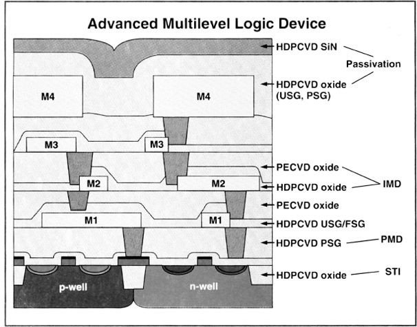
Multilayer Metal Scheme
The increase in chip density allows more devices to be placed on the wafer surface, which in turn reduces the area available for surface wiring. The solution to this dilemma is the multilayer metallization scheme (as shown in the figure below). By 2012, the International Technology Roadmap for Semiconductors (ITRS) predicted that there would be 15 to 20 metal layers.
A basic dual - metal stack is shown in the figure below. The stack starts with a barrier layer formed by siliciding the silicon surface to reduce the electrical contact resistance between the surface and the next layer. The barrier layer can also prevent the alloying of aluminum and silicon if pure aluminum is used as the conductive material. Next is a layer of dielectric material, called the inter - metal dielectric layer (IDL or IMD), which provides electrical isolation between metal layers. This dielectric can be a deposited oxide, silicon nitride, or a polyimide film.
This layer undergoes a photolithography step to etch new contact holes, called vias or plugs, all the way down to the first - layer metal. Conductive plugs are created by depositing conductive materials into the holes. Then, the second - layer metal is deposited and patterned. If there are subsequent layers, the IMD/plug/metal deposition or patterning sequence is repeated. Multilayer metal systems are more costly, have lower yields, and require more attention to the planarization of the wafer surface and intermediate layers to create good current - carrying leads.
Conductive Materials
Aluminum
This section discusses the three main materials used for metal interconnect layers. Before the emergence of very - large - scale integration (VLSI) circuits, the main metallization material was pure aluminum. Choosing aluminum and understanding its limitations can help us comprehend the general nature of metallization systems. From the perspective of electrical conductivity, aluminum is less conductive than copper and gold. If copper is directly used as a substitute for aluminum, it has high contact resistance with silicon and can cause severe damage to device performance if it enters the device area. Aluminum became the preferred metal because it avoids the above - mentioned problems.
It has a sufficiently low resistivity (2.7 micro - ohm·cm), good current - density carrying capacity, excellent adhesion to silicon dioxide, can be obtained in high purity, has low natural contact resistance with silicon, and is relatively easy to pattern using traditional photolithography processes. Aluminum sources are purified to a purity of 5 to 6 "nines" (99.999% to 99.9999%).
Aluminum - Silicon Alloy
The shallow junctions on the wafer surface present the first problem with using pure aluminum leads. The issue is the need to bake the aluminum - silicon interface to stabilize the electrical contact. This type of contact is called an ohmic contact because its voltage - current characteristic follows Ohm's law. Unfortunately, aluminum and silicon dissolve into each other and reach a eutectic formation point at 577°C. When the two materials are heated in contact, eutectic formation occurs at a temperature much lower than their respective melting points.
Eutectic formation occurs within a certain temperature range, and aluminum - silicon eutectic starts to form at around 450°C, which is also the temperature required for good electrical contact. The problem (usually called "spiking") is particularly severe at shallow junctions. If the alloy region is deep, it may completely penetrate the junction and short - circuit it (as shown in the figure below).
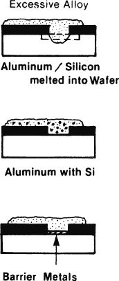
There are two solutions. One is the barrier metal layer (see the section on barrier metals), which separates aluminum and silicon to prevent eutectic alloy formation. The second is an alloy of aluminum with 1% to 2% silicon. During the contact heating step, aluminum alloys more with the silicon in the alloy rather than with the silicon in the wafer. This process is not 100% effective, and some alloying between aluminum and the wafer will always occur.
AMTD provides high - precision Showerhead services for core components. Its products mainly include semiconductor equipment core parts such as Shower head, Face plate, Blocker Plate, Top Plate, Shield, Liner, pumping ring, and Edge Ring. These products are widely used in fields such as semiconductors and display panels, with excellent performance and high market recognition.
Information source: WeChat official account FindRF
上一篇:Semiconductor Metallization: Deposition and Standards for Single - Layer Systems (Part 1)
下一篇:Key Process Processing Technologies in Semiconductor Fab


