


The chip manufacturing process is divided into two main parts. First, this part mainly involves fabricating the active and passive components of devices on the wafer surface, which is known as the Front - End - Of - Line (FEOL) process. Second, this part is concerned with connecting the devices and different layers through a metal system, known as the Back - End - Of - Line (BEOL) process. In the following section, we will introduce the materials, specifications, and methods used for metallization, as well as other applications of metals in chip manufacturing. The principle of vacuum pumps (used in Chemical Vapor Deposition (CVD), ion implantation, evaporation, and sputtering systems) is explained at the end of this chapter.
The most common use of metal thin films in semiconductor technology is for surface wiring. Conventionally, the materials, methods, and processes used to connect various parts of devices are collectively referred to as the metallization process. Moreover, depending on the complexity and performance requirements of the devices, circuits may require a single - layer metal system or a multi - layer system. Additionally, they may use aluminum alloy or copper as the conductive metal.
Deposition Methods
Sputtering of Aluminum Alloy and Other Metals
Low - Pressure Chemical Vapor Deposition (CVD) for Polysilicon, Tungsten, and Other Refractory Metals
Dual Damascene Process for Copper Electroplating
Metallization technology, like other manufacturing processes, has continuously evolved and improved with the emergence of new circuit requirements and materials. By the mid - 1970s, the main methods for metal deposition were vacuum evaporation of aluminum, gold, and fuse metals for Programmable Read - Only Memory (PROM) devices. The advent of multi - layer metal systems and alloys, as well as the demand for better step coverage, prompted sputtering to become the standard deposition technique for Very Large - Scale Integration (VLSI) manufacturing. The use of refractory metals introduced a second technique for metallization engineers, namely Chemical Vapor Deposition (CVD).
With the development of the dual damascene process and electroplating, copper was introduced as the primary metal.
The development of multi - layer systems has led to the emergence of barrier and adhesion layers, plugs, and inter - layer dielectric layers. The fundamentals of single - layer and multi - layer metal systems will be explored below.
Single - Layer Metal System
In the era of Medium - Scale Integration (MSI), metallization was relatively simple (as shown in the figure below), requiring only a single - layer metal process. Small holes, called contact holes, are etched through a photolithography step (known as contact photolithography) down to the contact areas on individual devices. After contact photolithography, a thin layer of conductive metal (currently about 0.5 microns) is deposited over the entire wafer using vacuum evaporation, sputtering, or CVD techniques.
Unwanted portions are removed through traditional photolithography and etching processes or lift - off processes, leaving the surface covered with thin metal lines known as leads, metal wires, or interconnects. Usually, a thermal treatment step called alloying is performed after metal patterning to ensure good electrical contact between the metal and the wafer surface. This basic process is illustrated in the figure below.
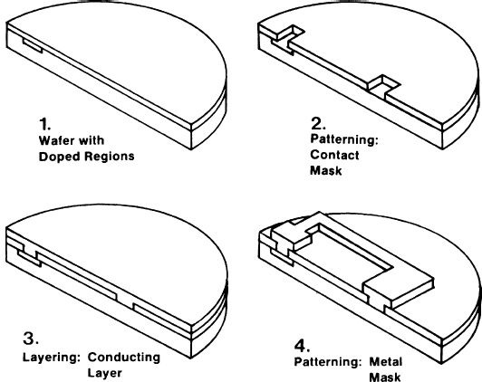
Figure 1
Regardless of the structure, the metal system must meet the following standards:
Good current - carrying capacity (current density)
Good adhesion to the wafer surface (usually silicon dioxide)
Ease of patterning
Good electrical contact with the wafer materials
High purity
Corrosion resistance
Long - term stability
Ability to deposit a uniform film free of voids and hills
Uniform grain structure
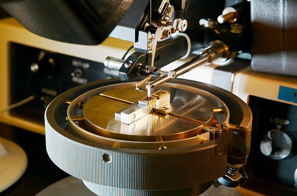
Anhui Boxinwei Semiconductor Technology Co., Ltd. provides high - precision Showerhead services for core components. Its products mainly include semiconductor equipment core parts such as Shower head, Face plate, Blocker Plate, Top Plate, Shield, Liner, pumping ring, and Edge Ring. These products are widely applied in fields including semiconductors and display panels, with excellent performance and high market recognition.
AMTD provides high - precision Showerhead services for core components. Its products mainly include semiconductor equipment core parts such as Shower head, Face plate, Blocker Plate, Top Plate, Shield, Liner, pumping ring, and Edge Ring. These products are widely applied in fields including semiconductors and display panels. With outstanding performance, they enjoy high market recognition.
Information source: WeChat official account FindRF
上一篇:Introduction to Four Thin - Film Deposition Technologies: PVD, ALD, LPCVD, and PECVD
下一篇:Semiconductor Metallization: Deposition and Standards for Single - Layer Systems (Part 2)


