

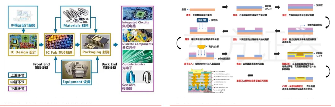
Semiconductor equipment is the core of the upstream semiconductor industry chain. It plays a crucial role in chip manufacturing and serves as the cornerstone and foundation of the semiconductor manufacturing industry. Wafer manufacturing equipment represents the largest demand in the semiconductor equipment industry, with equipment investment accounting for a significant portion of capital expenditures in wafer fabs. Lithography, etching, and thin-film deposition equipment are particularly important. Various types of semiconductor equipment are required throughout the semiconductor production process. In the IC manufacturing process, wafer manufacturing includes silicon wafer production and wafer processing. The former involves a series of steps such as single crystal growth, crystal processing, slicing, grinding, chamfering, and polishing, while the latter includes steps such as oxidation, photoresist coating, and lithography, among others. Semiconductor equipment is utilized in these corresponding steps. After the IC manufacturing process, the wafers with embedded integrated circuits, which have not yet been diced, enter the IC assembly and test (A&T) phase. This includes a series of steps such as wafer grinding, dicing, die bonding, and so on. Corresponding semiconductor assembly and test equipment are used in each step to ultimately produce the finished chip.
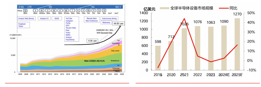
The global semiconductor equipment market is expected to rebound, with optimistic demand from growth-oriented industries. The semiconductor industry is not only cyclical but also a growth industry, where technological upgrades and product innovations are direct drivers of increased demand. Driven by strong demand from emerging application areas such as 5G, the Internet of Things, smart cars, cloud computing, big data, medical electronics, and security electronics, medium to long-term demand remains optimistic. In 2023, global semiconductor equipment sales experienced a slight decline, but a strong rebound is expected by 2025. According to data from the Semiconductor Industry Association (SEMI), global semiconductor manufacturing equipment sales fell slightly by 1.3% in 2023, from the record high of 107.5billionin2022to106.3 billion. SEMI states that the total investment in the semiconductor equipment market will reach 109billionin2024,withfront−endequipmentinvestmentaccountingfor98 billion, or 90% of the total, and back-end assembly and test investment totaling $11 billion, or 10% of the overall market.
It is projected that the total size of the global semiconductor equipment market will grow by 16% in 2025, with all segments achieving double-digit growth, pushing the equipment market size to exceed $127 billion, setting a new record.
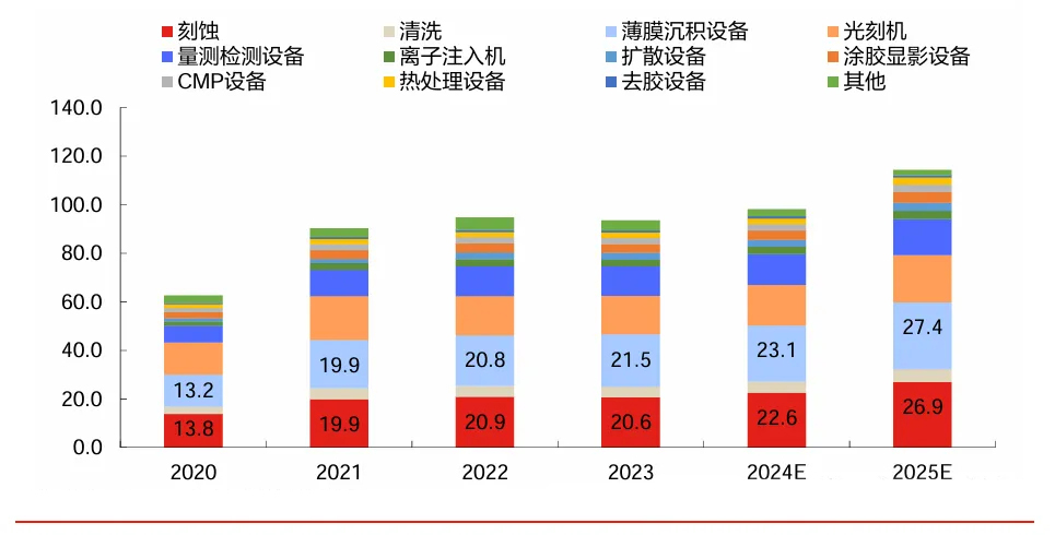
All segments of the market are expected to maintain growth, with thin-film deposition and etching equipment accounting for the largest share. It is forecasted that the global semiconductor equipment market will reach 127billionin2025,withthin−filmdepositionequipmentandetchingequipmentaccountingforthehighestmarketshares,at27.4 billion and $26.9 billion respectively.
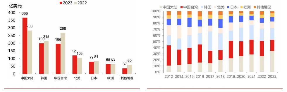
China's market is the largest globally and maintains high growth. Mainland China is the world's largest semiconductor equipment market and maintains the fastest growth rate, with its share of the global market continuously increasing and showing a trend of sustained growth. The semiconductor industry is expanding into Mainland China, offering vast opportunities for localization in design, manufacturing, equipment, and other segments. Throughout the development history of the global semiconductor industry, it has undergone several rounds of industrial transfers from the United States to Japan, then to South Korea, and subsequently to Taiwan, China, and Mainland China. Currently, Mainland China is in the midst of a rapid rise in industries such as smart electric vehicles, the Internet of Things, and artificial intelligence, and has become the world's most important semiconductor application and consumption market. In 2023, semiconductor equipment investment in Mainland China increased by 29% year-on-year, reaching $36.6 billion, and Mainland China's share of the global market rose to 34%.
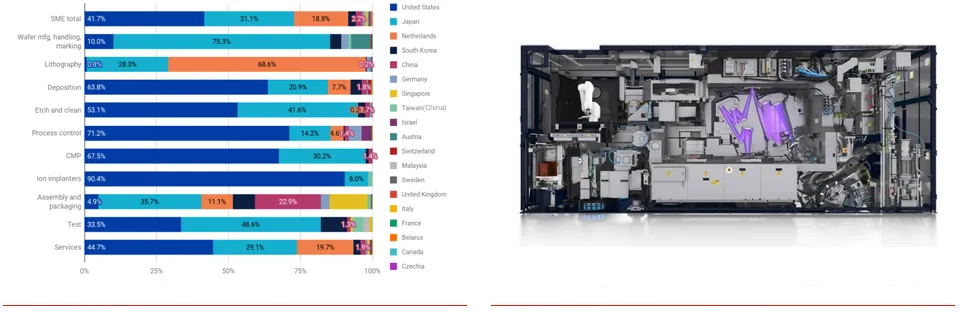
Advanced technologies still await breakthroughs, with significant barriers in technology and customer validation. Advanced technologies are dominated by countries such as the United States, Europe, and Japan, with the US, the Netherlands, and Japan holding competitive advantages in different equipment sectors. Specifically, the US leads the world in manufacturing technologies for etching equipment, ion implantation machines, thin-film deposition equipment, testing equipment, process control, CMP, and more. The Netherlands, with ASML's high-end lithography machines, occupies a leading position globally. Japan, on the other hand, has competitive advantages in etching equipment, cleaning equipment, and testing equipment. The semiconductor equipment industry is characterized by high technological barriers, stringent requirements for stable operation, and challenging customer validation processes, which are costly, time-consuming, and subject to rigorous standards. Due to the complexity of the equipment itself and the production line configuration, the yield and stability of individual pieces of equipment can have a cumulative effect within the entire system, potentially leading to substantial losses. Therefore, wafer manufacturers impose strict standards and procedures for the validation and acceptance of upstream equipment. For wafer fabs, cooperating in upstream equipment validation requires significant manpower (collaborative R&D, debugging), material resources (opportunity costs of allocating other equipment for validation, material losses during the validation process), and the enormous potential risks associated with adopting new equipment suppliers (risk of batch wafer scrap, risk of delayed delivery to customers).
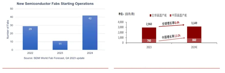
The underlying logic behind the sustained growth of the semiconductor equipment market is the increasing demand for semiconductors driven by the development of the technology industry, with the direct driving factor being the expansion of downstream wafer manufacturing fabs. Global wafer capacity continues to grow, with China leading the world in 2024 with a growth rate of 13% in wafer capacity. According to the SEMI report, following a 5.5% growth rate in 2023 to reach 29.6 million wafers per month, global semiconductor capacity is expected to increase by 6.4% in 2024, surpassing the 30 million wafers per month mark. Driven by government and other incentive measures, China's mainland region is expected to expand its share of global semiconductor capacity, with 18 new wafer fabs coming online throughout the year, and the capacity growth rate increasing from 12% in 2023 to 13% in 2024, with monthly capacity rising from 7.6 million wafers to 8.6 million wafers.
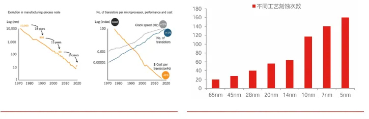
Technology upgrades drive the expansion of the semiconductor equipment industry. Moore's Law propels industry development, and the barriers in the equipment industry will continue to rise. According to the evolution of Moore's Law, chip performance doubles every 18-24 months. Advanced process IC capacity is experiencing robust growth, and according to IC Insights' forecast, the IC capacity of advanced processes (<10 nm) is expected to increase in 2024, reaching 30% of global capacity. With each new generation of process technology, a new generation of more advanced processing equipment is required. More sophisticated processes bring about a sharp increase in the difficulty of semiconductor equipment, continuously raising industry barriers. As processes advance and technologies upgrade, the demand for equipment per unit of capacity will further increase, and the investment per unit of capacity for advanced processes will rise exponentially. Process and technology upgrades drive an increase in chip complexity, and more complex structures require more manufacturing steps to complete, significantly increasing the usage of various types of equipment. Taking the etching process as an example, the number of etching steps required for the 14nm process reaches 64, while the 7nm process requires 140 etching steps, an increase of 118% compared to 14nm.
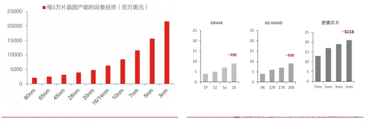
The investment per unit of capacity for advanced processes is increasing exponentially. As technology nodes continue to shrink, the equipment investment in integrated circuit manufacturing is showing a significant upward trend. The investment cost for the 5nm technology node reaches as high as $15.6 billion, more than double that of the 14nm node. The largest capital expenditure for a newly built production line comes from semiconductor equipment, with wafer manufacturing equipment accounting for 65% of the total capital expenditure for the new line.
The country provides strong support, and the third phase of the National Integrated Circuit Industry Investment Fund has been established. The country vigorously supports the development of the semiconductor equipment industry. In June 2014, with the approval of the State Council, the Ministry of Industry and Information Technology, together with relevant departments, released the "National Integrated Circuit Industry Development Promotion Outline," which explicitly established the National Integrated Circuit Industry Investment Fund. The aim is to support the R&D, production, and application of the domestic integrated circuit industry through capital investment, promote collaborative development across the industry chain, enhance China's competitiveness in the global semiconductor industry, drive the development of the semiconductor industry, and improve the country's self-reliance in key technology areas.
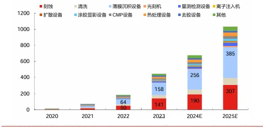
Geopolitical uncertainty poses high risks, making domestic substitution imperative. In the current complex and ever-changing international situation, geopolitical factors are increasingly impacting the global semiconductor industry. Trade frictions and technology blockades continue to occur, posing significant challenges to the stability of the semiconductor supply chain. Especially for a major semiconductor consumer like China, over-reliance on imported semiconductor equipment and products not only poses economic risks but also creates hidden dangers at the national strategic security level. Currently, Chinese semiconductor equipment manufacturers cover multiple sub-sectors, and the localization rate is expected to increase. With the growing emphasis on the semiconductor industry in China, a significant influx of capital, talent, and policy resources has followed. Chinese semiconductor equipment manufacturers continue to make technological breakthroughs in key sub-sectors such as etchers, lithography machines, and thin-film deposition equipment. As the localization rate of domestic semiconductor equipment increases, the market size of domestic equipment manufacturers is expected to grow rapidly. With the continuous improvement in the localization rate across various sub-sectors of semiconductor equipment, it is expected that by 2025, the localization rates for etching, cleaning, thin-film deposition, thermal processing, and photoresist stripping equipment will exceed 50%. Among these, the market sizes for etching equipment and thin-film deposition equipment will both exceed RMB 30 billion, and the market space for domestic semiconductor equipment manufacturers is expected to exceed RMB 100 billion.
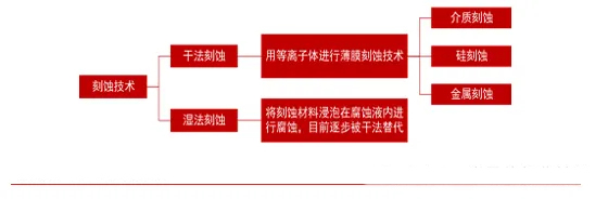
Etching technology is the core of chip manufacturing, with semiconductor equipment playing a critical role in this process. Wafer fabrication equipment, including etching equipment, deposition equipment, and lithography equipment, is one of the areas with the highest demand in the semiconductor equipment industry. As a core technology in integrated circuit (IC) manufacturing, etching technology primarily functions by removing excess oxide layers or other thin-film layers through ion bombardment and accurately transferring the circuit pattern from the photoresist film to the wafer surface. The etching machine industry chain can be divided into upstream, midstream, and downstream segments. The upstream segment includes vacuum chambers, etching chambers, gas supply systems, and vacuum systems; the midstream segment covers the manufacturing of etching machines; and the downstream segment primarily includes semiconductor devices and other micromechanical manufacturing. Within this industry chain, the manufacturing of etching equipment is the most critical link. Currently, many semiconductor devices adopt a mesa structure design, and the methods for mesa formation and etching equipment manufacturing can be categorized into wet etching and dry etching.
Etching technology is the core of chip manufacturing, with semiconductor equipment playing a critical role in this process. Wafer fabrication equipment, including etching equipment, deposition equipment, and lithography equipment, is one of the areas with the highest demand in the semiconductor equipment industry. As a core technology in integrated circuit (IC) manufacturing, etching technology primarily functions by removing excess oxide layers or other thin-film layers through ion bombardment and accurately transferring the circuit pattern from the photoresist film to the wafer surface. The etching machine industry chain can be divided into upstream, midstream, and downstream segments. The upstream segment includes vacuum chambers, etching chambers, gas supply systems, and vacuum systems; the midstream segment covers the manufacturing of etching machines; and the downstream segment primarily includes semiconductor devices and other micromechanical manufacturing. Within this industry chain, the manufacturing of etching equipment is the most critical link. Currently, many semiconductor devices adopt a mesa structure design, and the methods for mesa formation and etching equipment manufacturing can be categorized into wet etching and dry etching.
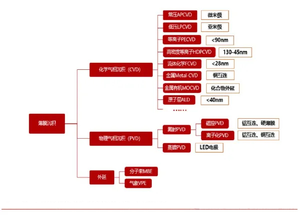
The segments of cleaning equipment and thermal processing equipment continue to expand. Vertical furnaces and cleaning equipment each account for approximately 5% of the total capital expenditure on integrated circuit equipment, playing pivotal roles in the integrated circuit production line. Vertical furnaces primarily include vertical oxidation/annealing furnaces, multi-wafer vertical low-pressure chemical vapor deposition (LPCVD) equipment, and multi-wafer vertical atomic layer deposition (ALD) equipment. Cleaning equipment mainly comprises single-wafer cleaning equipment and batch cleaning equipment. In 2023, the combined revenue of the company's vertical furnaces and cleaning equipment exceeded RMB 3 billion. In the field of cleaning equipment, batch cleaning machines have achieved full process coverage, while single-wafer cleaning machines have made new breakthroughs in advanced front-end processes, opening up a broader market space for the cleaning business segment. Through years of technological accumulation, Naura Technology Group has successively broken through multiple key module design technologies and cleaning process technologies, including Bernoulli chucks and double-sided process chucks, high-efficiency chemical recycling systems, hot SPM processes, hot phosphoric acid processes, low-pressure drying processes, etc. It has achieved full coverage of batch processes and made breakthroughs in high-end single-wafer processes. The company's process equipment in the integrated circuit field has been mass-produced at client sites. As of the end of 2023, the cumulative shipments of the company's cleaning equipment have exceeded 1,200 units.


