


The semiconductor supply chain reported at the end of last year that TSMC's 2nm trial production yield exceeded 60%, better than expected, and is on track for mass production in 2025. A netizen claiming to be a TSMC employee posted on a social media platform that TSMC is expanding its 2nm production capacity with a goal of producing over 100,000 wafers per month.
Previously, this newspaper disclosed that TSMC's 2nm process adopts a nanosheet architecture for the first time, which is more technically demanding and complex than the current 3nm FinFET process technology. Risk production is currently underway at the Baoshan Fab 1 in the Hsinchu Science Park, and once the yield reaches mass production standards, the mass production experience will be replicated at the first factory in Kaohsiung for mass production.
TSMC does not disclose the trial production yield, only emphasizing that the 2nm process is progressing smoothly and is on track for mass production in 2025, when it will be the industry's leading technology. The semiconductor supply chain has reported that TSMC's 2nm trial production yield exceeds 60%, better than expected.
Recently, it was reported that TSMC's 2nm monthly production capacity is expected to reach 50,000 wafers by the end of the year, and could potentially reach 80,000 wafers if progress goes smoothly. In response to these rumors, a netizen claiming to be a TSMC employee, Dr. Kim, posted on the social media platform X that the information is true, and stated, "We are expanding 2nm production capacity with a goal of producing over 100,000 wafers per month."
2nm: The Peak Competition
In addition to TSMC, Samsung and Intel are also making strides in 2nm technology.
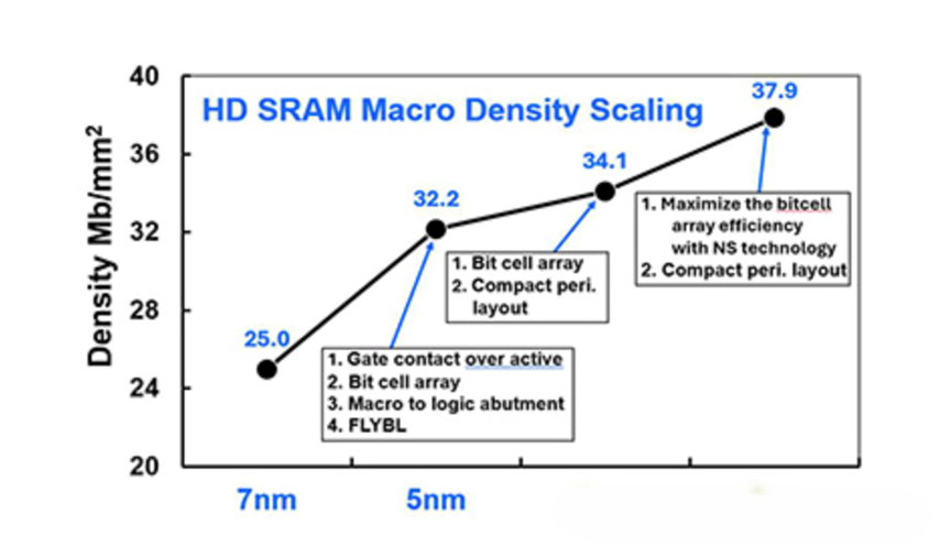
According to the renowned analysis firm TechInsights, Intel's 18A can offer higher performance, while TSMC's N2 may offer higher transistor density. TechInsights analysts believe that TSMC's N2 offers a high-density (HD) standard cell transistor density of 313 MTr/mm², significantly exceeding the HD cell densities of Intel's 18A (238 MTr/mm²) and Samsung's SF2/SF3P (231 MTr/mm²). Although this information generally aligns with the SRAM cell sizes of 18A, N2, and N3, as well as TSMC's expectations for N2 and N3, there are still some points to consider.
Firstly, this only pertains to HD standard cells. Almost all modern high-performance processors relying on cutting-edge nodes use a mix of high-density (HD), high-performance (HP), and low-power (LP) standard cells, not to mention features like TSMC's FinFlex and NanoFlex.
Secondly, it is currently unclear how Intel's and TSMC's HP and LP standard cells compare. While it is reasonable to assume that N2 leads in transistor density, its lead may not be as significant as that of HD standard cells. Thirdly, in papers presented at the IEDM event, both Intel and TSMC disclosed the performance, power, and transistor density advantages of their next-generation 18A and N2 manufacturing processes relative to their predecessor processes. However, there is currently no way to directly compare these two manufacturing technologies.
In terms of performance, TechInsights believes that Intel's 18A will lead TSMC's N2 and Samsung's SF2 (formerly known as SF3P). However, TechInsights uses a controversial method to compare the performance of upcoming nodes, as it benchmarks against TSMC's N16FF and Samsung's 14nm process technologies, and then adds the node-to-node performance improvements announced by the two companies to make predictions. While this may be an estimate, it may not be entirely accurate.
On the other hand, Intel focuses on manufacturing high-performance processors, so 18A can be tailored for performance and power efficiency rather than HD transistor density. Ultimately, 18A supports the backside power delivery network, PowerVia, and chips using this network may have performance and transistor density advantages over TSMC's N2, which does not support this feature. However, this does not mean that every 18A chip will use PowerVia.
When it comes to power consumption, TechInsights analysts speculate that chips based on N2 will consume less power than similar ICs based on SF2, as TSMC has been leading in power efficiency in recent years. As for Intel, this remains to be seen, but at least 18A will offer advantages in this aspect.
Another widely circulated figure is that the price per wafer for TSMC's 2nm process will reach $30,000.
TechInsights provides the world's leading semiconductor cost and price models. Before 3nm entered production,we estimated the cost per wafer to be less than 20,000,and some customers contacted us,insisting that the price for 3nm was 20,000 to 25,000 per wafer. After 3nm entered production,we were able to conduct proprietary for ensicanalysis of TSMC′sfinancial sand confirm that we wer ecorrect,with volume prices below 20,000per wafer, differing by thousands of dollars.
The jump from a price of less than 20,000per 3nm wafer to 30,000 per 2nm wafer represents more than a 1.5x increase, with a 1.15x increase in density, leading to a significant increase in transistor cost. This raises the question: who will pay for this? Our price estimate is less than $30,000 per wafer. There are also reports that Apple, typically TSMC's main customer for each node, may forgo initial use of 2nm due to price, although we have also heard opposing views.
Another element of this discussion is that TSMC's prices for high-volume wafers are much lower than those for low-volume wafers, so volume needs to be considered in any discussion. Overall, we believe that $30,000 is higher than the average pricing for high volumes.
If TSMC sets the price for 2nm wafers at $30,000 per wafer, they will put significant pressure on customers, forcing them to turn to Intel and Samsung for 2nm-class wafer supplies.
Source: Content compiled from Semiconductor Industry Observations.


