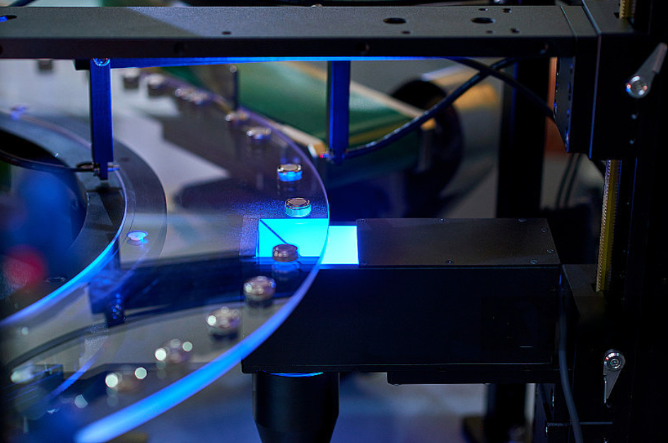


In the field of thin - film deposition technology, PVD (Physical Vapor Deposition), ALD (Atomic Layer Deposition), LPCVD (Low - Pressure Chemical Vapor Deposition), and PECVD (Plasma - Enhanced Chemical Vapor Deposition) are four important technologies that play crucial roles in their respective areas. Below is a detailed introduction to these four technologies.
I. PVD (Physical Vapor Deposition)
1. Definition and Classification
PVD is a technology for preparing thin films by physically evaporating or sputtering materials from a source onto a substrate surface. It mainly includes various methods such as evaporation coating, sputtering coating, ion plating, and pulsed laser deposition.
2. Basic Principles and Process Flow
The basic principle of PVD technology is to utilize the impact of high - speed particles to evaporate or sputter materials from the source onto the substrate surface, forming a thin film. The specific process flow includes material evaporation or sputtering, plasma generation (in ion plating and sputtering coating), thin - film deposition, and thin - film growth. By controlling parameters such as evaporation rate, target power, substrate temperature, and gas pressure, it is possible to precisely control the thickness and composition of the thin film.
3. Advantages and Disadvantages
The advantages of PVD technology lie in its ability to deposit high - quality thin films at low temperatures, its applicability to a wide range of materials, and its high adhesion and uniformity. However, the equipment is complex and expensive, a high - vacuum environment is required during the process, and there are certain limitations on the shape and size of the substrate.
4. Typical Application Cases
In semiconductor manufacturing, PVD technology is used to deposit metal interconnect layers and diffusion barrier layers, improving device performance. In the field of hard coatings, it can form wear - resistant coatings on the surfaces of tools and molds, extending their service life. In the field of optical thin films, it is used to manufacture anti - reflection films, filters, etc., enhancing the performance of optical devices.
II. ALD (Atomic Layer Deposition)
1. Definition and Working Principle
ALD is a thin - film deposition technology based on self - limiting surface reactions, capable of precisely controlling the thickness and composition of thin films at the atomic level. It deposits thin films layer by layer on the substrate surface by alternately introducing different precursor gases.
2. Comparison with CVD
Compared with CVD, ALD, with its self - limiting reaction characteristics, can achieve higher - precision and more uniform thin - film control. In contrast, CVD has advantages in terms of deposition rate and process flexibility.
3. Advantages and Disadvantages
The advantages of ALD technology include its extremely high precision and uniformity, its applicability to nano - scale structures and substrates with complex shapes, and the high quality of the deposited thin films. However, its deposition rate is relatively low, the selection of precursors and process control are complex, and the cost is high.
4. Applications in Modern Industry
ALD technology has a wide range of applications in fields such as nano - materials, battery technology, and biomedical applications. In the field of nano - materials, it is used to prepare nano - scale functional materials, enhancing their performance and application scope. In battery technology, it can form high - performance electrode and electrolyte thin films in lithium - ion batteries, improving battery capacity and lifespan. In biomedical applications, it is used to form functional thin films on the surfaces of biosensors and medical devices, improving their biocompatibility and performance.
III. LPCVD (Low - Pressure Chemical Vapor Deposition)
1. Definition and Working Principle
LPCVD is a technology for precisely laying various thin - film materials on the surface of chips by controlling chemical reactions in a low - pressure environment. It generates high - quality and extremely uniform thin films by precisely regulating the chemical reactions of precursors under low pressure.
2. Advantages and Disadvantages
The advantages of LPCVD technology lie in its ability to generate high - quality and extremely uniform thin films, making it suitable for chip manufacturing and the deposition of other high - temperature materials. However, it requires a high - temperature environment, and the equipment maintenance requirements are high.
3. Typical Application Cases
In chip manufacturing, LPCVD technology is used to prepare important insulating and protective layers such as silicon oxide and silicon nitride, as well as doped thin films. These thin films are not only the foundation of the circuit structure but also crucial for the performance and reliability of the chips.
IV. PECVD (Plasma - Enhanced Chemical Vapor Deposition)
1. Definition and Working Principle
PECVD is a technology for depositing thin films at low temperatures by exciting gas decomposition reactions through plasma. It enhances the chemical activity of reactive substances and promotes chemical reactions between gases by means of low - temperature plasma generated by gas glow discharge, thus forming new solid films on the substrate at low temperatures.
2. Advantages and Disadvantages
The advantage of PECVD technology is its ability to deposit thin films at low temperatures, making it suitable for heat - sensitive materials. However, the quality of the formed film may be affected by factors such as plasma uniformity and substrate temperature.
3. Typical Application Cases
In electronic devices, PECVD technology is used to prepare silicon nitride insulating layers,
low - temperature optical thin films, etc. In addition, in the photovoltaic field, PECVD technology is also used to prepare passivation layers and anti - reflection layers in PERC batteries and TOPCon batteries.
AMTD provides high - precision Showerhead services for core components. Its products mainly include semiconductor equipment core parts such as Shower head, Face plate, Blocker Plate, Top Plate, Shield, Liner, pumping ring, and Edge Ring. These products are widely applied in fields including semiconductors and display panels. With outstanding performance, they enjoy high market recognition.
This article is compiled with reference to the following materials:
1. From Basic Principles to Industrial Practice | Process Flow and Application Highlights of PVD Coating Technology
2. ALD, a Very Valuable Technology
3. ALD Technology Special Report: Weidao Nano Based on ALD Layout in Photovoltaic & Semiconductor, Expanding CVD to Open Up Growth Space
4. Analysis of TOPCon Core Process Technology Routes and Production Line Costs
5. Low - Pressure Chemical Vapor Deposition (LPCVD) (The core information about LPCVD in this article is referenced from relevant sections of this material)
6. Panoramic View of Thin - Film Deposition Methods, Analysis of Three Major Processes and Equipment to Assist in the Preparation of Efficient Materials (Part of the information about PECVD in this article is referenced from relevant content of this material)
上一篇:Common Machining Processes
下一篇:Semiconductor Metallization: Deposition and Standards for Single - Layer Systems (Part 1)